SLVSBY8D May   2013  – June 2020 TPS2513 , TPS2513A , TPS2514 , TPS2514A

PRODUCTION DATA.  

  1. Features
  2. Applications
  3. Description
    1.     Device Images
      1.      Simplified Schematic
  4. Revision History
  5. Device Options
  6. Pin Configuration and Functions
    1.     Pin Functions: TPS2513x
    2.     Pin Functions: TPS2514x
  7. Specifications
    1. 7.1 Absolute Maximum Ratings
    2. 7.2 ESD Ratings
    3. 7.3 Recommended Operating Conditions
    4. 7.4 Thermal Information
    5. 7.5 Electrical Characteristics
    6. 7.6 Typical Characteristics
  8. Detailed Description
    1. 8.1 Overview
    2. 8.2 Functional Block Diagrams
    3. 8.3 Feature Description
      1. 8.3.1 Dedicated Charging Port (DCP)
      2. 8.3.2 Short the D+ Line to the D– Line
      3. 8.3.3 Divider DCP
      4. 8.3.4 Applying 1.2 V to the D+ Line and 1.2 V to the D– Line
      5. 8.3.5 DCP Auto-Detect
      6. 8.3.6 Undervoltage Lockout (UVLO)
    4. 8.4 Device Functional Modes
  9. Applications and Implementation
    1. 9.1 Application Information
    2. 9.2 Typical Applications
      1. 9.2.1 Design Requirements
      2. 9.2.2 Detailed Design Procedure
        1. 9.2.2.1 Divide Mode Selection of 5-W and 10-W USB Chargers
      3. 9.2.3 Application Curves
  10. 10Power Supply Recommendations
  11. 11Layout
    1. 11.1 Layout Guidelines
    2. 11.2 Layout Example
  12. 12Device and Documentation Support
    1. 12.1 Related Links
    2. 12.2 Receiving Notification of Documentation Updates
    3. 12.3 Support Resources
    4. 12.4 Trademarks
    5. 12.5 Electrostatic Discharge Caution
    6. 12.6 Glossary
  13. 13Mechanical, Packaging, and Orderable Information

Package Options

Mechanical Data (Package|Pins)
Thermal pad, mechanical data (Package|Pins)
Orderable Information

Divider DCP

There are three charging schemes for divider DCP. They are named after Divider 1, Divider 2, and Divider 3 DCPs that are shown in Figure 11, Figure 12, and Figure 13. The Divider 1 charging scheme is used for 5-W adapters, and applies 2 V to the D+ line and 2.7 V to the D– data line. The Divider 2 charging scheme is used for 10-W adapters, and applies 2.7 V on the D+ line and 2 V is applied on the D– line. The Divider 3 charging scheme is used for 12-W adapters, and applies 2.7 V on D+ and D– lines.
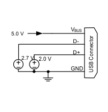
TPS2513 TPS2513A TPS2514 TPS2514A fig010_lvsby8.gifFigure 11. Divider 1 DCP
TPS2513 TPS2513A TPS2514 TPS2514A divide_3_mode_slusby8.gifFigure 13. Divider 3 DCP
TPS2513 TPS2513A TPS2514 TPS2514A fig011_lvsby8.gifFigure 12. Divider 2 DCP