SLVSCU5 March 2015 TPS25200-Q1
PRODUCTION DATA.
- 1 Features
- 2 Applications
- 3 Description
- 4 Simplified Schematic
- 5 Revision History
- 6 Pin Configuration and Functions
- 7 Specifications
- 8 Parameter Measurement Information
- 9 Detailed Description
- 10Application and Implementation
- 11Power Supply Recommendations
- 12Layout
- 13Device and Documentation Support
- 14Mechanical, Packaging, and Orderable Information
Package Options
Mechanical Data (Package|Pins)
- DRV|6
Thermal pad, mechanical data (Package|Pins)
- DRV|6
Orderable Information
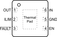
6 Pin Configuration and Functions
DRV Package
6-Pin WSON With Exposed Thermal Pad
Top View

Pin Functions
| PIN | I/O | DESCRIPTION | |
|---|---|---|---|
| NAME | NO. | ||
| EN | 4 | I | Logic-level control input. When this pin is driven high, the power switch is enabled. When this pin is driven low, the power switch turns off. This pin cannot be left floating and it must be limited below the absolute maximum rating if tied to the IN pin. |
| FAULT | 3 | O | Active-low open-drain output. This pin is asserted during an overcurrent, overvoltage, or overtemperature event. Connect a pullup resistor to the logic I/O voltage. |
| GND | 5 | — | Ground connection. Connect this pin externally to the exposed thermal pad. |
| ILIM | 2 | O | External resistor. The ILIM pin is used to set the current-limit threshold. The recommended value for this pin is: 36 kΩ ≤ RILIM ≤ 1100 kΩ. |
| IN | 6 | I | Input voltage. Connect a ceramic capacitor with a value of 0.1 μF or greater from the IN pin to the GND pin as close to the IC as possible. |
| OUT | 1 | O | Protected power switch, VOUT. |
| Thermal pad | — | The exposed thermal pad is internally connected to the GND pin. Use the thermal pad to heat-sink the device to the circuit board traces. Connect the thermal pad to the GND pin externally. | |