SLVSCJ0E March 2014 – June 2021 TPS25200
PRODUCTION DATA
- 1 Features
- 2 Applications
- 3 Description
- 4 Revision History
- 5 Pin Configuration and Functions
- 6 Specifications
- 7 Parameter Measurement Information
- 8 Detailed Description
- 9 Application and Implementation
- 10Power Supply Recommendations
- 11Layout
- 12Device and Documentation Support
- 13Mechanical, Packaging, and Orderable Information
Package Options
Mechanical Data (Package|Pins)
- DRV|6
Thermal pad, mechanical data (Package|Pins)
- DRV|6
Orderable Information
3 Description
The TPS25200 is a 5-V eFuse with precision current limit and overvoltage clamp. The device provides robust protection for load and source during overvoltage and overcurrent events.
The TPS25200 is an intelligent protected load switch with VIN tolerant to 20 V. In the event that an incorrect voltage is applied at IN, the output clamps to 5.4 V to protect the load. If the voltage at IN exceeds 7.6 V, the device disconnects the load to prevent damage to the device and/or load.
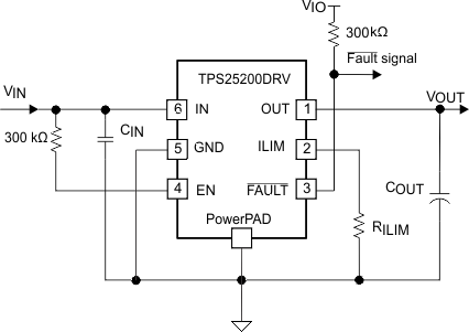
The TPS25200 has an internal 60-mΩ power switch and is intended for protecting source, device, and load under a variety of abnormal conditions. The device provides up to 2.5 A of continuous load current. Current limit is programmable from 85 mA to 2.9 A with a single resistor to ground. During overload events output current is limited to the level set by RILIM. If a persistent overload occurs the device eventually goes into thermal shutoff to prevent damage to the TPS25200.
| ORDER NUMBER | PACKAGE | BODY SIZE |
|---|---|---|
| TPS25200 | WSON (6) | 2.00 mm × 2.00 mm |
 Simplified Schematic
 VOUT vs
VIN