SLVSCJ0E March 2014 – June 2021 TPS25200
PRODUCTION DATA
- 1 Features
- 2 Applications
- 3 Description
- 4 Revision History
- 5 Pin Configuration and Functions
- 6 Specifications
- 7 Parameter Measurement Information
- 8 Detailed Description
- 9 Application and Implementation
- 10Power Supply Recommendations
- 11Layout
- 12Device and Documentation Support
- 13Mechanical, Packaging, and Orderable Information
Package Options
Mechanical Data (Package|Pins)
- DRV|6
Thermal pad, mechanical data (Package|Pins)
- DRV|6
Orderable Information
9.2.3 Application Curves
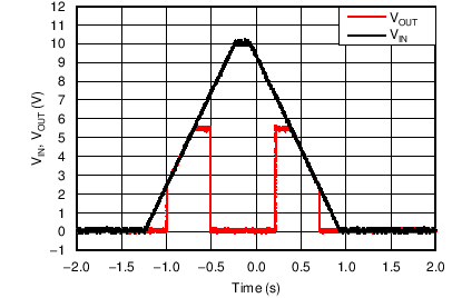 Figure 9-6 VOUT vs VIN (0 V to 10 V)
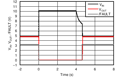 Figure 9-8 Pulse Overvoltage with
100 Ω
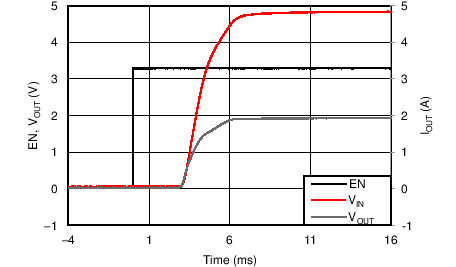 Figure 9-10 Turnon Delay and Rise Time 150 µF || 2.5 Ω
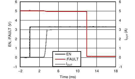 Figure 9-12 Enable into Output Short
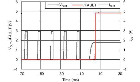 Figure 9-14 Output Short to 2.5-Ω Load Recovery Response
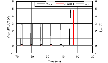 Figure 9-16 Output Short to No Load Recovery Response
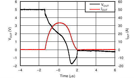 Figure 9-18 50-mΩ Hot-Short Response Time
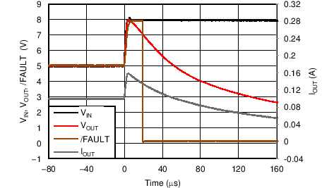 Figure 9-7 VIN Step 5 V
to 8 V with 4.7 μF // 100 Ω
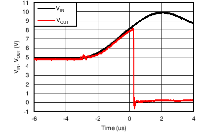 Figure 9-9 5-V to 10-V OVLO Response
Time
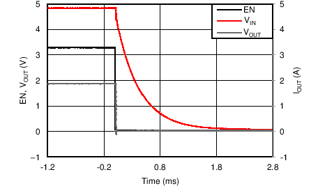 Figure 9-11 Turnoff Delay and Fall Time 150 µF || 2.5 Ω
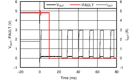 Figure 9-13 2.5 Ω to Output Short Transient Response
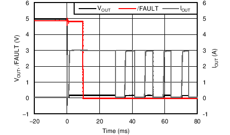 Figure 9-15 No Load to Output Short Transient Response
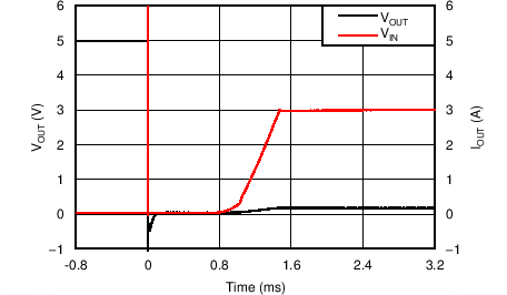 Figure 9-17 Hot-Short With 50 mΩ