SLVSCA1B October   2013  – August 2016 TPS2546-Q1

PRODUCTION DATA.  

  1. Features
  2. Applications
  3. Description
  4. Revision History
  5. Pin Configuration and Functions
  6. Specifications
    1. 6.1 Absolute Maximum Ratings
    2. 6.2 ESD Ratings
    3. 6.3 Recommended Operating Conditions
    4. 6.4 Thermal Information
    5. 6.5 Electrical Characteristics
    6. 6.6 Electrical Characteristics: High-Bandwidth Switch
    7. 6.7 Electrical Characteristics: Charging Controller
    8. 6.8 Typical Characteristics
  7. Parameter Measurement Information
  8. Detailed Description
    1. 8.1 Overview
    2. 8.2 Functional Block Diagram
    3. 8.3 Feature Description
      1. 8.3.1  Standard Downstream Port (SDP) USB 2.0/USB 3.0
      2. 8.3.2  Charging Downstream Port (CDP)
      3. 8.3.3  Dedicated Charging Port (DCP)
        1. 8.3.3.1 DCP BC1.2 and YD/T 1591-2009
        2. 8.3.3.2 DCP Divider Charging Scheme
        3. 8.3.3.3 DCP 1.2-V Charging Scheme
      4. 8.3.4  Wake on USB Feature (Mouse/Keyboard Wake Feature)
        1. 8.3.4.1 USB 2.0 Background Information
        2. 8.3.4.2 Wake On USB
        3. 8.3.4.3 USB Slow-Speed and Full-Speed Device Recognition
          1. 8.3.4.3.1 No CTL Pin Timing Requirement After Wake Event and Transition from S3 to S0
      5. 8.3.5  Load Detect
      6. 8.3.6  Power Wake
        1. 8.3.6.1 Implementing Power Wake in Notebook System
      7. 8.3.7  Port Power Management (PPM)
        1. 8.3.7.1 Benefits of PPM
        2. 8.3.7.2 PPM Details
        3. 8.3.7.3 Implementing PPM in a System with Two Charging Ports
      8. 8.3.8  Overcurrent Protection
      9. 8.3.9  FAULT Response
      10. 8.3.10 Undervoltage Lockout (UVLO)
      11. 8.3.11 Thermal Sense
    4. 8.4 Device Functional Modes
      1. 8.4.1 DCP Auto Mode
      2. 8.4.2 DCP Forced Shorted / DCP Forced Divider1
      3. 8.4.3 High-Bandwidth Data Line Switch
      4. 8.4.4 Device Truth Table (TT)
  9. Application and Implementation
    1. 9.1 Application Information
      1. 9.1.1 Output Discharge
      2. 9.1.2 CDP/SDP Auto Switch
    2. 9.2 Typical Application
      1. 9.2.1 Design Requirements
      2. 9.2.2 Detailed Design Procedure
        1. 9.2.2.1 Current-Limit Settings
      3. 9.2.3 Application Curves
  10. 10Power Supply Recommendations
  11. 11Layout
    1. 11.1 Layout Guidelines
    2. 11.2 Layout Example
  12. 12Device and Documentation Support
    1. 12.1 Documentation Support
      1. 12.1.1 Related Documentation
    2. 12.2 Receiving Notification of Documentation Updates
    3. 12.3 Community Resources
    4. 12.4 Trademarks
    5. 12.5 Electrostatic Discharge Caution
    6. 12.6 Glossary
  13. 13Mechanical, Packaging, and Orderable Information

Package Options

Mechanical Data (Package|Pins)
Thermal pad, mechanical data (Package|Pins)
Orderable Information

7 Parameter Measurement Information
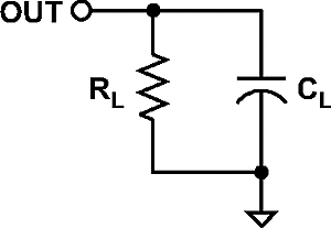
TPS2546-Q1 rise_fall_tst_lvsba6.gif Figure 23. Out Rise/Fall Test Load
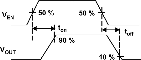
TPS2546-Q1 pwr_on_off_lvsba6.gif Figure 24. Power-ON and OFF Timing
TPS2546-Q1 enable_tim_lvsba6.gif Figure 25. Enable Timing, Active High Enable
TPS2546-Q1 discharge_lvsba6.gif Figure 26. Out Discharge During Mode Change
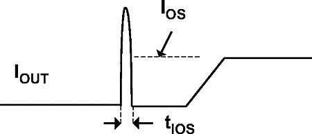
TPS2546-Q1 op_short_cir_lvsba6.gif Figure 27. Output Short-Circuit Parameters