SLUSCE3C October   2015  – August 2020 TPS2549-Q1

PRODUCTION DATA  

  1. Features
  2. Applications
  3. Description
  4. Revision History
  5. Pin Configuration and Functions
  6. Specifications
    1. 6.1 Absolute Maximum Ratings
    2. 6.2 ESD Ratings
    3. 6.3 Recommended Operating Conditions
    4. 6.4 Thermal Information
    5. 6.5 Electrical Characteristics
    6. 6.6 Switching Characteristics
    7. 6.7 Typical Characteristics
  7. Parameter Measurement Information
  8. Detailed Description
    1. 8.1 Overview
    2. 8.2 Functional Block Diagram
    3. 8.3 Feature Description
      1. 8.3.1  FAULT Response
      2. 8.3.2  Cable Compensation
        1. 8.3.2.1 Design Procedure
      3. 8.3.3  D+ and D– Protection
      4. 8.3.4  Output and D+ or D– Discharge
      5. 8.3.5  Port Power Management (PPM)
        1. 8.3.5.1 Benefits of PPM
        2. 8.3.5.2 PPM Details
        3. 8.3.5.3 Implementing PPM in a System With Two Charging Ports (CDP and SDP1)
        4. 8.3.5.4 Implementing PPM in a System With Two Charging Ports (DCP and DCP1)
      6. 8.3.6  CDP and SDP Auto Switch
      7. 8.3.7  Overcurrent Protection
      8. 8.3.8  Undervoltage Lockout
      9. 8.3.9  Thermal Sensing
      10. 8.3.10 Current Limit Setting
    4. 8.4 Device Functional Modes
      1. 8.4.1 Device Truth Table (TT)
      2. 8.4.2 USB Specification Overview
      3. 8.4.3 Standard Downstream Port (SDP) Mode — USB 2.0 and USB 3.0
      4. 8.4.4 Charging Downstream Port (CDP) Mode
      5. 8.4.5 Dedicated Charging Port (DCP) Mode
        1. 8.4.5.1 DCP BC1.2 and YD/T 1591-2009
        2. 8.4.5.2 DCP Divider-Charging Scheme
        3. 8.4.5.3 DCP 1.2-V Charging Scheme
      6. 8.4.6 DCP Auto Mode
      7. 8.4.7 Client Mode
      8. 8.4.8 High-Bandwidth Data-Line Switches
  9. Application and Implementation
    1. 9.1 Application Information
    2. 9.2 Typical Application
      1. 9.2.1 Design Requirements
      2. 9.2.2 Detailed Design Procedure
        1. 9.2.2.1 Input and Output Capacitance
        2. 9.2.2.2 Cable Compensation Calculation
        3. 9.2.2.3 Power Dissipation and Junction Temperature
    3. 9.3 Application Curves
  10. 10Power Supply Recommendations
  11. 11Layout
    1. 11.1 Layout Guidelines
    2. 11.2 Layout Example
  12. 12Device and Documentation Support
    1. 12.1 Documentation Support
      1. 12.1.1 Related Documentation
    2. 12.2 Receiving Notification of Documentation Updates
    3. 12.3 Support Resources
    4. 12.4 Trademarks
    5. 12.5 Electrostatic Discharge Caution
    6. 12.6 Glossary
  13. 13Mechanical, Packaging, and Orderable Information

Package Options

Mechanical Data (Package|Pins)
Thermal pad, mechanical data (Package|Pins)
Orderable Information

Typical Characteristics

GUID-72FFBFFD-B3E7-4C46-AD22-629A065CACC2-low.gif
VIN = 5 V
Figure 6-1 Power Switch On-Resistance vs Temperature
GUID-1E60C67D-4F21-4DF8-A7B6-A972D86D7FE2-low.gif
Figure 6-3 OUT Discharge Resistance vs Temperature
GUID-8B2804EC-1080-4561-894B-FA8EA6D6D9C6-low.gif
CTL1 = 1 CTL2 = 1 CTL3 = 1
Figure 6-5 Disabled IN Supply Current vs Temperature
GUID-3DFCF17C-2969-4021-BE8A-1EE65A756F56-low.gif
CTL1 = 0 CTL2 = 0 CTL3 = 1
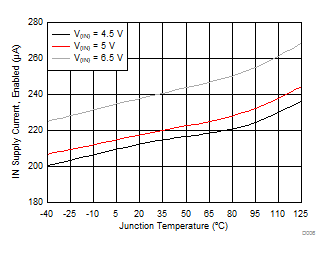
Figure 6-7 Enabled IN Supply Current – DCP_Auto (001) vs Temperature
GUID-43EB31D5-6E46-4A4A-A2BE-975D99A67561-low.gif
CTL1 = 1 CTL2 = 0 CTL3 = 0
Figure 6-9 Enabled IN Supply Current – Client Mode (100) vs Temperature
GUID-7BDB6F72-DE6D-4FC5-A8CF-1791BA02DD9F-low.gif
VIN = 5 V
Figure 6-11 DP_IN Overvoltage Protection Threshold vs Temperature
GUID-A0A99FEE-4CD8-4E1D-8EE3-48FDECC5E66F-low.gif
VIN = 5 V VCS = 2. 5 V
Figure 6-13 ICS vs Temperature
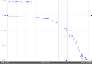
GUID-1E8C2FE5-6618-465D-9A31-ADE2293B98C7-low.gifFigure 6-15 Data Transmission Characteristics vs Frequency
GUID-DCCE59DC-4C30-46D0-9E69-743FC92EFA89-low.gifFigure 6-17 On-State Cross-Channel Isolation vs Frequency
GUID-F45169A9-E793-4381-B2EC-AF3A1C98AF61-low.gif
VIN = 5 V
Figure 6-2 Reverse Leakage Current vs Temperature
GUID-8E0EFC1C-8FB8-40C9-B7F9-4C9C39CD3D65-low.gif
VIN = 5 V
Figure 6-4 OUT Short-Circuit Current Limit vs Temperature
GUID-1123ED92-BD7B-48D9-B1C5-9EF27FBA217C-low.gif
CTL1 = 1 CTL2 = 1 CTL3 = 1
Figure 6-6 Enabled IN Supply Current – CDP (111) vs Temperature
GUID-2254B8F5-A8C8-46CE-873F-D2612929392B-low.gif
CTL1 = 0 CTL2 = 1 CTL3 = 0
Figure 6-8 Enabled IN Supply Current – SDP (010) vs Temperature
GUID-5EC628B5-8334-493B-B6AB-B560005029F6-low.gif
R(ILIM_LO) = 80.6 kΩ
Figure 6-10 IOUT Rising Load-Detect Threshold and OUT Short-Circuit Current Limit vs Temperature
GUID-121A3E14-2FF5-4694-A89D-93DB3EE6A7E0-low.gif
VIN = 5 V
Figure 6-12 DM_IN Overvoltage Protection Threshold vs Temperature
GUID-F0C914B0-D41E-4973-877B-A344EFE9EB77-low.gif
VIN = 6.5 V
Figure 6-14 ICS vs VCS Voltage
GUID-EE672D7F-874C-43B2-8629-CFFAFCB22C47-low.gifFigure 6-16 Off-State Data-Switch Isolation vs Frequency

GUID-42547298-B4C1-47D4-BA42-41BDC428EAEF-low.gifFigure 6-18 Eye Diagram Using USB Compliance Test Pattern, Bypassing the TPS2549-Q1 Data Switch
GUID-C4D6F3D5-E2FA-4302-961F-E7C12DF477EE-low.gif
R(LOAD) = 5 Ω C(LOAD) = 150 µF t = 1 ms/div
Figure 6-20 Turnon Response
GUID-4A9F49AD-0145-4BBF-9E7B-42821A5153E1-low.gif
R(ILIM_HI) = 80.6 kΩ t = 2 ms/div
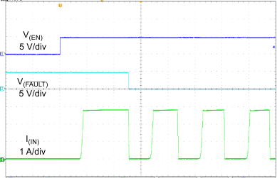
Figure 6-22 Enable Into Short
GUID-EC93C11A-1E76-490E-ABD8-AD5FBD7ED523-low.gif
R(ILIM_HI) = 19.1 kΩ t = 4 ms/div
Figure 6-24 Short-Circuit to Full-Load Recovery
GUID-EBBF9F35-3684-4FAF-AB8E-220A2DCC2302-low.gif
R(ILIM_HI) = 19.1 kΩ R(SHORT) = 50 mΩ t = 1 ms/div
Figure 6-26 Hot Short
GUID-8EA68739-E727-4F14-84C0-9023D3F3A500-low.gif
R(ILIM_LO) = 80.6 kΩ t = 1 s/div
Figure 6-28 Load Detection Reset Time
GUID-E66BF5BB-9A39-4133-8004-2D013FC8CC0B-low.gif
R(DM_OUT) = 15 kΩ t = 4 ms/div
Figure 6-30 DM_IN Short to VBUS
GUID-16B880C0-194E-48BC-A342-B43043FE71A4-low.gifFigure 6-19 Eye Diagram Using USB Compliance Test Pattern, Through the TPS2549-Q1 Data Switch
GUID-87E0B762-C259-4641-B14A-4C6597B6CDD4-low.gif
R(LOAD) = 5 Ω C(LOAD) = 150 µF t = 1 ms/div
Figure 6-21 Turnoff Response
GUID-BFE66FA6-A257-4173-888B-F73F07838470-low.gif
R(ILIM_HI) = 19.1 kΩ t = 4 ms/div
Figure 6-23 Enable Into Short – Thermal Cycling
GUID-C0921184-BBE3-4785-8A6B-1977EFAEAEEE-low.gif
R(SHORT) = 50 mΩ t = 1 µs/div
Figure 6-25 Hot-Short Response Time
GUID-740ACAFB-1FDE-4D49-92BF-E4C2C6F0EDEC-low.gif
R(ILIM_LO) = 80.6 kΩ t = 100 ms/div
Figure 6-27 Load-Detection Set Time
GUID-B97056ED-DB94-4A71-858F-A6B7EF45F911-low.gif
R(DM_OUT) = 15 kΩ t = 1 µs/div
Figure 6-29 DM_IN Short to VBUS Response Time
GUID-F240504B-03D2-43BC-9042-084A44C7F5CE-low.gif
R(DM_OUT) = 15 kΩ t = 1 µs/div
Figure 6-31 DM_IN Short-to-VBUS Recovery