SLVS850A June   2008  – September 2023 TPS2551-Q1

PRODUCTION DATA  

  1.   1
  2. Features
  3. Applications
  4. Description
  5. Revision History
  6. Pin Configurations and Functions
  7. Specifications
    1. 6.1 Absolute Maximum Ratings
    2. 6.2 ESD Ratings
    3. 6.3 Recommended Operating Conditions
    4. 6.4 Thermal Information
    5. 6.5 Electrical Characteristics
    6. 6.6 Typical Characteristics
  8. Parameter Measurement Information
  9. Detailed Description
    1. 8.1 Overview
    2. 8.2 Functional Block Diagram
    3. 8.3 Feature Description
      1. 8.3.1 Overcurrent
      2. 8.3.2 Reverse-Voltage Protection
      3. 8.3.3 FAULT Response
      4. 8.3.4 Undervoltage Lockout (UVLO)
      5. 8.3.5 Enable (EN)
      6. 8.3.6 Thermal Sense
      7. 8.3.7 Device Functional Modes
    4. 8.4 Programming
      1. 8.4.1 Programming the Current-Limit Threshold
  10. Application and Implementation
    1. 9.1 Application Information
    2. 9.2 Typical Application
      1. 9.2.1 Two-Level Current-Limit Circuit
      2. 9.2.2 Design Requirements
      3. 9.2.3 Detail Design Procedure
        1. 9.2.3.1 Designing Above a Minimum Current Limit
        2. 9.2.3.2 Designing Below a Maximum Current Limit
        3. 9.2.3.3 Input and Output Capacitance
      4. 9.2.4 Auto-Retry Functionality
      5. 9.2.5 Latch-Off Functionality
      6. 9.2.6 Typical Application as USB Power Switch
        1. 9.2.6.1 Design Requirements
          1. 9.2.6.1.1 USB Power-Distribution Requirements
        2. 9.2.6.2 Detail Design Procedure
          1. 9.2.6.2.1 Universal Serial Bus (USB) Power-Distribution Requirements
    3. 9.3 Power Supply Recommendations
      1. 9.3.1 Self-Powered and Bus-Powered Hubs
      2. 9.3.2 Low-Power Bus-Powered and High-Power Bus-Powered Functions
      3. 9.3.3 Power Dissipation and Junction Temperature
    4. 9.4 Layout
      1. 9.4.1 Layout Guidelines
      2. 9.4.2 Layout Example
  11. 10Device and Documentation Support
    1. 10.1 Receiving Notification of Documentation Updates
    2. 10.2 Support Resources
    3. 10.3 Trademarks
    4. 10.4 Electrostatic Discharge Caution
    5. 10.5 Glossary
  12. 11Mechanical, Packaging, and Orderable Information

Package Options

Mechanical Data (Package|Pins)
Thermal pad, mechanical data (Package|Pins)
Orderable Information

Latch-Off Functionality

The circuit in Figure 9-4 uses an SN74HC00 quad-NAND gate to implement overcurrent latch-off. The SN74HC00 high-speed CMOS logic gate is selected because it operates over the 2.5-V to 6.5-V range of the TPS2551.

This circuit is designed to work with the active-high TPS2551. ENABLE must be logic low during start-up until VIN is stable to ensure that the switch initializes in the OFF state. A logic high on ENABLE turns on the switch after VIN is stable. FAULT momentarily pulls low during an overcurrent condition, which latches STAT logic low and disables the switch. The host can monitor STAT for an overcurrent condition. Toggling ENABLE resets STAT and re-enables the switch.
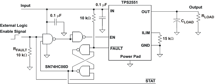
GUID-1252434C-3BF7-4DEB-ACD4-B5DE231DFA2E-low.gifFigure 9-4 Overcurrent Latch-Off Using a Quad-NAND Gate