SLVSBD0B November   2012  – June 2020 TPS2553-Q1

PRODUCTION DATA.  

  1. Features
  2. Applications
  3. Description
    1.     Device Images
      1.      Typical Application as USB Power Switch
  4. Revision History
  5. Pin Configuration and Functions
    1.     Pin Functions
  6. Specifications
    1. 6.1 Absolute Maximum Ratings
    2. 6.2 ESD Ratings
    3. 6.3 Recommended Operating Conditions
    4. 6.4 Thermal Information
    5. 6.5 Electrical Characteristics
    6. 6.6 Typical Characteristics
  7. Parameter Measurement Information
  8. Detailed Description
    1. 8.1 Overview
    2. 8.2 Functional Block Diagram
    3. 8.3 Feature Description
      1. 8.3.1 Overcurrent Conditions
      2. 8.3.2 Reverse-Voltage Protection
      3. 8.3.3 FAULT Response
      4. 8.3.4 Undervoltage Lockout (UVLO)
      5. 8.3.5 Enable (EN)
      6. 8.3.6 Thermal Sense
    4. 8.4 Device Functional Modes
    5. 8.5 Programming
      1. 8.5.1 Programming the Current-Limit Threshold
  9. Application and Implementation
    1. 9.1 Application Information
      1. 9.1.1 Constant-Current and Impact on Output Voltage
      2. 9.1.2 Accounting for Resistor Tolerance
      3. 9.1.3 Input and Output Capacitance
    2. 9.2 Typical Applications
      1. 9.2.1 Application 1: Designing Above a Minimum Current-Limit
        1. 9.2.1.1 Design Requirements
        2. 9.2.1.2 Detailed Design Procedure
        3. 9.2.1.3 Application Curves
      2. 9.2.2 Application 2: Designing Below a Maximum Current-Limit
        1. 9.2.2.1 Design Requirements
        2. 9.2.2.2 Detailed Design Procedure
      3. 9.2.3 Application 3: Auto-Retry Functionality
        1. 9.2.3.1 Design Requirements
        2. 9.2.3.2 Detailed Design Procedure
      4. 9.2.4 Application 4: Two-Level Current-Limit Circuit
        1. 9.2.4.1 Design Requirements
        2. 9.2.4.2 Detailed Design Procedure
      5. 9.2.5 Application 5: Typical Application as USB Power Switch
        1. 9.2.5.1 Design Requirements
        2. 9.2.5.2 Detailed Design Procedure
          1. 9.2.5.2.1 Universal Serial Bus (USB) Power-Distribution Requirements
  10. 10Power Supply Recommendations
    1. 10.1 USB Self-Powered (SPH) and Bus-Powered (BPH) Hubs
    2. 10.2 USB Low-Power Bus-Powered and High-Power Bus-Powered Functions
  11. 11Layout
    1. 11.1 Layout Guidelines
    2. 11.2 Layout Example
    3. 11.3 Power Dissipation and Junction Temperature
  12. 12Device and Documentation Support
    1. 12.1 Device Support
    2. 12.2 Support Resource
    3. 12.3 Trademarks
    4. 12.4 Electrostatic Discharge Caution
    5. 12.5 Glossary
  13. 13Mechanical, Packaging, and Orderable Information

Package Options

Refer to the PDF data sheet for device specific package drawings

Mechanical Data (Package|Pins)
  • DBV|6
Thermal pad, mechanical data (Package|Pins)
Orderable Information

Typical Characteristics

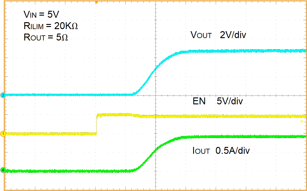
TPS2553-Q1 TURN ON DELAY.png
t =1 mS/div
Figure 1. Turnon Delay and Rise Time
TPS2553-Q1 EN TO SHORT.png
t =1 mS/div
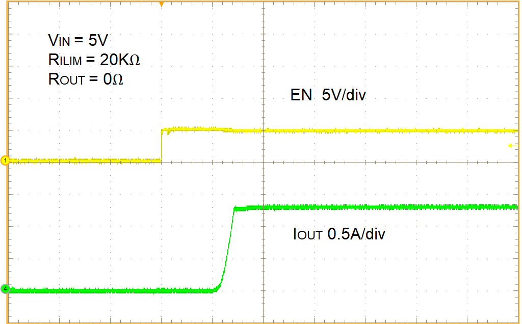
Figure 3. Device Enabled Into Short-Circuit
TPS2553-Q1 full_ld_rec_lvs841.gif
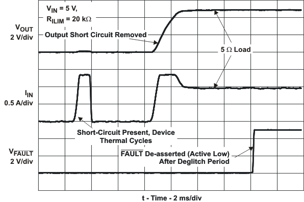
Figure 5. Short-Circuit to Full-Load Recovery Response
TPS2553-Q1 no_load_rec_lvs841.gif
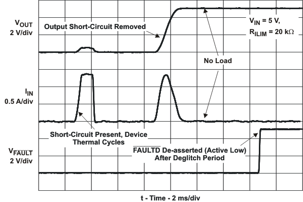
Figure 7. Short-Circuit to No-Load Recovery Response
TPS2553-Q1 trns_nl_1o_lvs841.gif
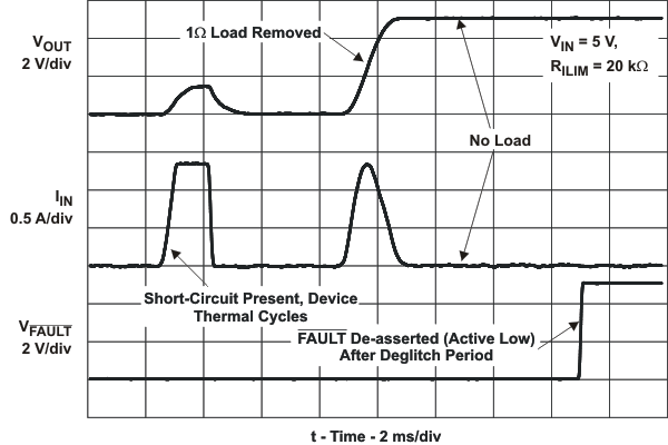
Figure 9. 1 Ω to No Load Transient Response
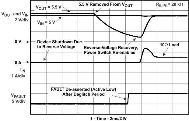
TPS2553-Q1 rev2_v_prot_lvsbd0.gif
Figure 11. Reverse-Voltage Protection Recovery
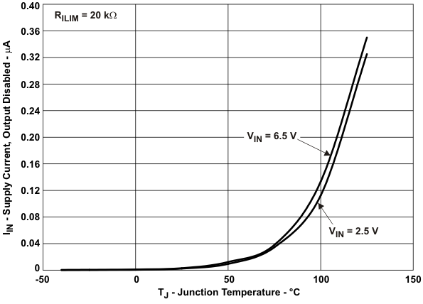
TPS2553-Q1 iin_tj_lvs841.gif
Figure 13. IIN – Supply Current, Output Disabled – μA
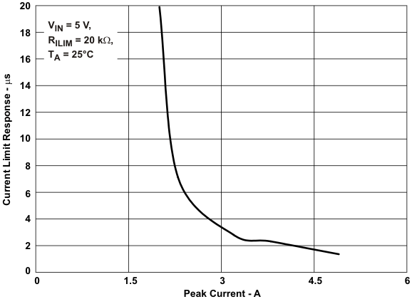
TPS2553-Q1 cl_pc_lvs841.gif
Figure 15. Current-Limit Response – μs
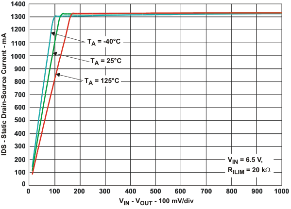
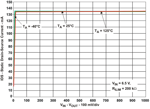
TPS2553-Q1 ids_vds_lvs841.gif
Figure 17. Switch Current Vs. Drain-Source Voltage Across Switch
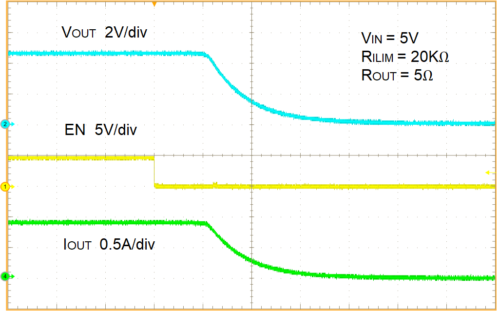
TPS2553-Q1 TURN OFF DELAY.png
t =1 mS/div
Figure 2. Turnoff Delay and Fall Time
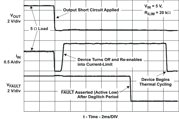
TPS2553-Q1 full_ld_lvs841.gif
Figure 4. Full-Load to Short-Circuit Transient Response
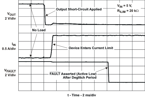
TPS2553-Q1 no_load_lvs841.gif
Figure 6. No-Load to Short-Circuit Transient Response
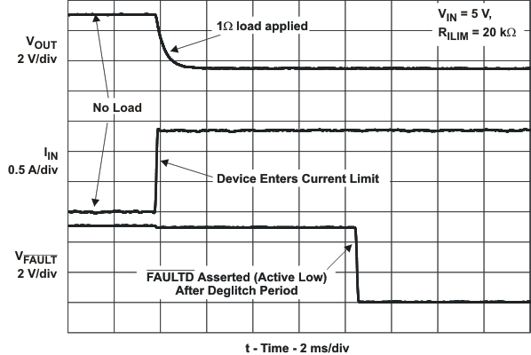
TPS2553-Q1 no_load_1o_lvs841.gif
Figure 8. No Load to 1-Ω Transient Response
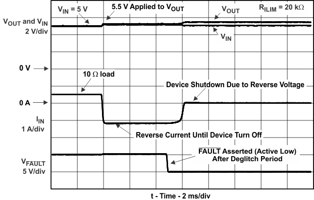
TPS2553-Q1 rev_v_prot_lvsbd0.gif
Figure 10. Reverse-Voltage Protection Response
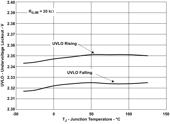
TPS2553-Q1 uvlo_tj_lvs841.gif
Figure 12. UVLO – Undervoltage Lockout – V
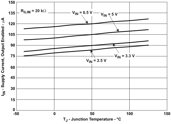
TPS2553-Q1 iin2_tj_lvs841.gif
Figure 14. IIN – Supply Current, Output Enabled – μA
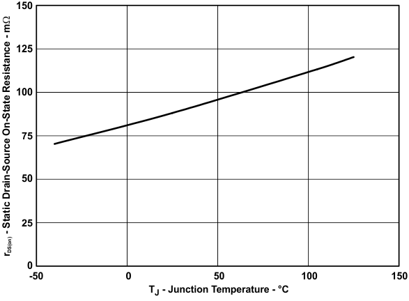
TPS2553-Q1 rdson_tj_lvsbd0.gif
Figure 16. MOSFET rDS(on) Vs. Junction Temperature
TPS2553-Q1 ids2_vds_lvs841.gif
Figure 18. Switch Current Vs. Drain-Source Voltage Across Switch