SLVSDJ5D August 2016 – January 2018 TPS25741 , TPS25741A
UNLESS OTHERWISE NOTED, this document contains PRODUCTION DATA.
- 1 Features
- 2 Applications
- 3 Description
- 4 Revision History
- 5 Device Comparison Table
- 6 Pin Configuration and Functions
- 7 Specifications
-
8 Detailed Description
- 8.1 Overview
- 8.2 Functional Block Diagram
- 8.3
Feature Description
- 8.3.1 USB Type-C CC Logic (CC1, CC2)
- 8.3.2 9.3.2 VCONN Supply (VCONN, CC1, CC2)
- 8.3.3 USB Power Delivery BMC Transmission (CC1, CC2, VTX)
- 8.3.4 USB Power Delivery BMC Reception (CC1, CC2)
- 8.3.5 Discharging (DSCG, VPWR)
- 8.3.6 Configuring Voltage Capabilities (HIPWR, EN9V, EN12V)
- 8.3.7 Configuring Power Capabilities (PSEL, PCTRL, HIPWR)
- 8.3.8 Gate Drivers
- 8.3.9 Fault Monitoring and Protection
- 8.3.10 Voltage Control (CTL1, CTL2)
- 8.3.11 Sink Attachment Indicator (UFP, DVDD)
- 8.3.12 Accessory Attachment Indicator (AUDIO, DEBUG)
- 8.3.13 Plug Polarity Indication (POL)
- 8.3.14 Power Supplies (VAUX, VDD, VPWR, DVDD)
- 8.3.15 Grounds (AGND, GND)
- 8.3.16 Output Power Supply (DVDD)
- 8.4 Device Functional Modes
- 9 Application and Implementation
- 10Power Supply Recommendations
- 11Layout
- 12Device and Documentation Support
- 13Mechanical, Packaging, and Orderable Information
Package Options
Mechanical Data (Package|Pins)
- RSM|32
Thermal pad, mechanical data (Package|Pins)
- RSM|32
Orderable Information
7.7 Switching Characteristics
Unless otherwise stated in a specific test condition the following conditions apply: –40°C ≤ TJ ≤ 125°C; 3.0 V ≤ VDD ≤ 5.5 V, 4.65 V ≤ VPWR ≤ 25 V; HIPWR = GND, PSEL = GND, GD = VAUX, PCTRL = VAUX, AGND = GND, EN9V = GND; EN12V = GND; VAUX, VTX, bypassed with 0.1 µF, DVDD bypassed with 0.22 µF; all other pins open (unless otherwise noted)| PARAMETER | TEST CONDITIONS | MIN | TYP | MAX | UNIT | |
|---|---|---|---|---|---|---|
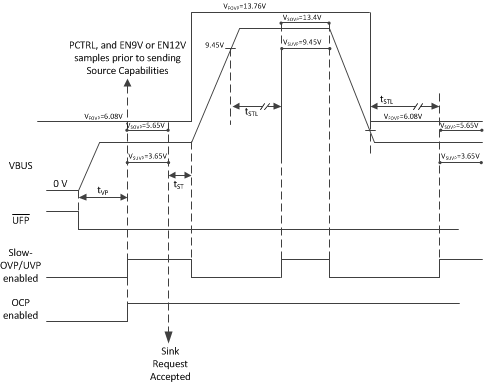
| tVP | Delay from enabling external NFET until under-voltage and OCP protection are enabled | VBUS = GND | 190 | ms | ||
| tSTL | Source settling time, time from CTL1 and CTL2 being changed until a PS_RDY USB Power Delivery message is transmitted to inform the sink is may draw full current per USB Power Delivery in Documentation Support. | 260 | ms | |||
| tSR | Time that VBUS is held low after a hard reset. This is tSrcRecover in USB Power Delivery in Documentation Support. | TJ > TJ1 | 765 | ms | ||
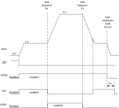
| tHR | Time after hard reset is transmitted until GDNG is disabled. This is tPSHardReset in USB Power Delivery in Documentation Support. | 30 | ms | |||
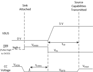
| tCCDeb | Time until UFP or AUDIO or DEBUG is pulled low after an attachment, this is the USB Type-C required debounce time for attachment detection called tCCDebounce [1]. | 185 | ms | |||
| tST | Delay after sink request is accepted until CTL1 and/or CTL2 is changed. This is called tSnkTransition in USB Power Delivery in Documentation Support. | 30 | ms | |||
| tFLT | The time in between hard reset transmissions in the presence of a persistent supply fault. | GD = GND or VPWR = GND, sink attached | 1395 | ms | ||
| tSH | The time in between retries (hard reset transmissions) in the presence of a persistent VBUS short. | VBUS = GND, sink attached | 985 | ms | ||
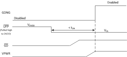
| tON | The time from UFP being pulled low until a hard reset is transmitted. Designed to be greater than tSrcTurnOn in USB Power Delivery in Documentation Support. | GD = 0 V or VPWR = 0 V | 600 | ms | ||
| Retry interval if USB Power Delivery sink stops communicating without being removed or if sink does not communicate after a fault condition. Time GDNG remains enabled before a hard reset is transmitted. This is the tNoResponse time in USB Power Delivery in Documentation Support. | Sink attached | 4.8 | s | |||
| tDVDD | Delay before DVDD is driven high | After sink attached | 5 | ms | ||
| tGDoff | Turnoff delay, time until VGDNG is below 10% of its initial value after the GD pin is low. | VGD: 5 V → 0 V in < 0.5 µs. | 5 | µs | ||
| tFOVP | Response time when VBUS exceeds the fast-OVP threshold | VBUS ↑ to GDNG OFF (VGDNG below 10% its initial value) |
30 | µs | ||
| OCP large signal response time | 5 A enabled, VISNS – VVBUS: 0 V → 42 mV measured to GDNG transition start. | 30 | µs | |||
| Time until discharge is stopped after TJ1 is exceeded. | 0 V ≤ VDSCG ≤ 25 V | 10 | µs | |||
| Digital output fall time | VPULLUP = 1.8 V, CLoad = 10 pF, RPULLUP = 10 kΩ, V(CTLx) or VUFP : 70% VPULLUP → 30% VPULLUP |
20 | 300 | ns | ||
| tVCON | VCONN turn-on time | Measured from when UFP is pulled low until VCONN FET is enabled. | 2 | ms | ||
| VBUS turn-on time | Measured from when UFP is pulled low until GDNG begins sourcing its full current | 2 | ms | |||
 Figure 1. Timing Diagram for tVP, tST, and tSTL, After Sink Attachment. VSOVP and VSUVP are Disabled Around Voltage Transitions
 Figure 2. Timing Diagram for tHR and tSR, After Sink Attachment with TJ > TJ1
 Figure 3. Timing Diagram for tCcDeb and tCD, Under Persistent Fault Condition
 Figure 4. Timing Diagram for tSH and tVP, with VBUS Shorted to Ground
 Figure 5. Timing Diagram for tON
 Figure 6. Timing Diagram for GDPG, G5V, and GDNG with Fast-Shutdown Fault