SLVSDJ5D August 2016 – January 2018 TPS25741 , TPS25741A
UNLESS OTHERWISE NOTED, this document contains PRODUCTION DATA.
- 1 Features
- 2 Applications
- 3 Description
- 4 Revision History
- 5 Device Comparison Table
- 6 Pin Configuration and Functions
- 7 Specifications
-
8 Detailed Description
- 8.1 Overview
- 8.2 Functional Block Diagram
- 8.3
Feature Description
- 8.3.1 USB Type-C CC Logic (CC1, CC2)
- 8.3.2 9.3.2 VCONN Supply (VCONN, CC1, CC2)
- 8.3.3 USB Power Delivery BMC Transmission (CC1, CC2, VTX)
- 8.3.4 USB Power Delivery BMC Reception (CC1, CC2)
- 8.3.5 Discharging (DSCG, VPWR)
- 8.3.6 Configuring Voltage Capabilities (HIPWR, EN9V, EN12V)
- 8.3.7 Configuring Power Capabilities (PSEL, PCTRL, HIPWR)
- 8.3.8 Gate Drivers
- 8.3.9 Fault Monitoring and Protection
- 8.3.10 Voltage Control (CTL1, CTL2)
- 8.3.11 Sink Attachment Indicator (UFP, DVDD)
- 8.3.12 Accessory Attachment Indicator (AUDIO, DEBUG)
- 8.3.13 Plug Polarity Indication (POL)
- 8.3.14 Power Supplies (VAUX, VDD, VPWR, DVDD)
- 8.3.15 Grounds (AGND, GND)
- 8.3.16 Output Power Supply (DVDD)
- 8.4 Device Functional Modes
- 9 Application and Implementation
- 10Power Supply Recommendations
- 11Layout
- 12Device and Documentation Support
- 13Mechanical, Packaging, and Orderable Information
Package Options
Mechanical Data (Package|Pins)
- RSM|32
Thermal pad, mechanical data (Package|Pins)
- RSM|32
Orderable Information
8.3.3 USB Power Delivery BMC Transmission (CC1, CC2, VTX)
An example of the BMC signal, specifically the end of the preamble and beginning of start-of-packet (SOP) is shown below. There is always an edge at the end of each bit or unit interval, and ones have an edge half way through the unit interval.
 Figure 25. BMC Encoded End of Preamble, Beginning of SOP
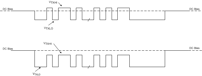
While engaging in USB Power Delivery communications, the TPS25741 or TPS25741A is applying IRP1.5 or IRP3.0, so the CC line has a DC voltage of 0.918 V or 1.68 V, respectively. When the BMC signal is transmitted on the CC line, the transmitter overrides this DC voltage as shown in Figure 26. The transmitter bias rail (VTX) is internally generated and may not be used for any other purpose in the system. The VTX pin is only high while the TPS25741 or TPS25741A is transmitting a USB Power Delivery message.
 Figure 26. USB Power Delivery BMC Transmission on the CC Line
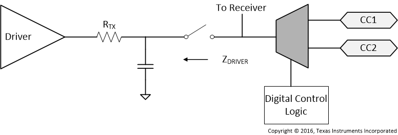
The device transmissions meet the eye diagram requirements from USB Power Delivery in Documentation Support. Figure 27 shows the transmitter schematic.
 Figure 27. USB Power Delivery BMC Transmitter Schematic
The transmit eye diagram shown in Figure 29 was measured using the test load shown in Figure 28 with a CLOAD within the allowed range. The total capacitance CLOAD is computed as:
Where:
- 200 pF < CRX < 600 pF
- CCablePlug < 25 pF
- Ca < 625 pF
- 200 pF < CReceiver < 600 pF
Therefore, 400 pF < CLOAD < 1850 pF.
 Figure 28. Test Load for BMC Transmitter
Figure 29 shows the transmit eye diagram for the TPS25741 and TPS25741A.
 Figure 29. Transmit Eye Diagram (BMC)
The transmitter bias rail (VTX) is internally generated and may not be used for any other purpose in the system. Connect a 0.1-µF capacitor to GND from this pin. The VTX pin is only high while the TPS25741/TPS25741A is transmitting a USB Power Delivery message.