SLVSDJ5D August 2016 – January 2018 TPS25741 , TPS25741A
UNLESS OTHERWISE NOTED, this document contains PRODUCTION DATA.
- 1 Features
- 2 Applications
- 3 Description
- 4 Revision History
- 5 Device Comparison Table
- 6 Pin Configuration and Functions
- 7 Specifications
-
8 Detailed Description
- 8.1 Overview
- 8.2 Functional Block Diagram
- 8.3
Feature Description
- 8.3.1 USB Type-C CC Logic (CC1, CC2)
- 8.3.2 9.3.2 VCONN Supply (VCONN, CC1, CC2)
- 8.3.3 USB Power Delivery BMC Transmission (CC1, CC2, VTX)
- 8.3.4 USB Power Delivery BMC Reception (CC1, CC2)
- 8.3.5 Discharging (DSCG, VPWR)
- 8.3.6 Configuring Voltage Capabilities (HIPWR, EN9V, EN12V)
- 8.3.7 Configuring Power Capabilities (PSEL, PCTRL, HIPWR)
- 8.3.8 Gate Drivers
- 8.3.9 Fault Monitoring and Protection
- 8.3.10 Voltage Control (CTL1, CTL2)
- 8.3.11 Sink Attachment Indicator (UFP, DVDD)
- 8.3.12 Accessory Attachment Indicator (AUDIO, DEBUG)
- 8.3.13 Plug Polarity Indication (POL)
- 8.3.14 Power Supplies (VAUX, VDD, VPWR, DVDD)
- 8.3.15 Grounds (AGND, GND)
- 8.3.16 Output Power Supply (DVDD)
- 8.4 Device Functional Modes
- 9 Application and Implementation
- 10Power Supply Recommendations
- 11Layout
- 12Device and Documentation Support
- 13Mechanical, Packaging, and Orderable Information
Package Options
Mechanical Data (Package|Pins)
- RSM|32
Thermal pad, mechanical data (Package|Pins)
- RSM|32
Orderable Information
8.3.1 USB Type-C CC Logic (CC1, CC2)
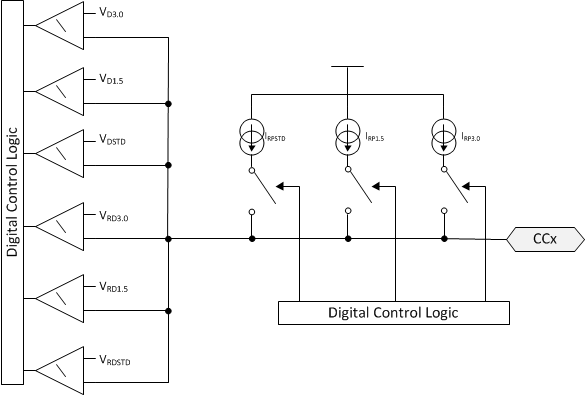
The TPS25741/TPS25741A uses a current source to implement the pull up resistance USB Type-C requires for Sources. While waiting for a valid connection, the TPS25741/TPS25741A applies a default pullup of IRPSTD. A sink attachment is detected when the voltage on one (not both) of the CC pins remains between VRDSTD and VDSTD for tCcDeb and the voltage on the VBUS pin is below VBUS_FTH. Then after turning on VBUS and disabling the Rp current source and applying VCONN to the CCx pin not connected through the cable, the TPS25741/TPS25741A applies IRP3.0 to advertise 3A to non-Power Delivery sinks. Finally, if it is determined that the attached sink is Power Delivery-capable, the TPS25741/TPS25741A applies IRP1.5. During this sequence if the voltage on the monitored CC pin exceeds the detach threshold then the TPS25741/TPS25741A removes VBUS and begins watching for a sink attachment again.
The TPS25741 or TPS25741A digital logic selects the current source switch as illustrated in Figure 23.
 Figure 23. USB Type-C Rp Current Sources and Detection Comparators
If the voltage on both CC pins remains above VRDSTD for tCcDeb, then the TPS25741 or TPS25741A goes to the sleep mode. In the sleep mode a less accurate current source is applied and less accurate comparator watches for attachment (see VWAKE, and IDSDFP).