SLVSDJ5D August 2016 – January 2018 TPS25741 , TPS25741A
UNLESS OTHERWISE NOTED, this document contains PRODUCTION DATA.
- 1 Features
- 2 Applications
- 3 Description
- 4 Revision History
- 5 Device Comparison Table
- 6 Pin Configuration and Functions
- 7 Specifications
-
8 Detailed Description
- 8.1 Overview
- 8.2 Functional Block Diagram
- 8.3
Feature Description
- 8.3.1 USB Type-C CC Logic (CC1, CC2)
- 8.3.2 9.3.2 VCONN Supply (VCONN, CC1, CC2)
- 8.3.3 USB Power Delivery BMC Transmission (CC1, CC2, VTX)
- 8.3.4 USB Power Delivery BMC Reception (CC1, CC2)
- 8.3.5 Discharging (DSCG, VPWR)
- 8.3.6 Configuring Voltage Capabilities (HIPWR, EN9V, EN12V)
- 8.3.7 Configuring Power Capabilities (PSEL, PCTRL, HIPWR)
- 8.3.8 Gate Drivers
- 8.3.9 Fault Monitoring and Protection
- 8.3.10 Voltage Control (CTL1, CTL2)
- 8.3.11 Sink Attachment Indicator (UFP, DVDD)
- 8.3.12 Accessory Attachment Indicator (AUDIO, DEBUG)
- 8.3.13 Plug Polarity Indication (POL)
- 8.3.14 Power Supplies (VAUX, VDD, VPWR, DVDD)
- 8.3.15 Grounds (AGND, GND)
- 8.3.16 Output Power Supply (DVDD)
- 8.4 Device Functional Modes
- 9 Application and Implementation
- 10Power Supply Recommendations
- 11Layout
- 12Device and Documentation Support
- 13Mechanical, Packaging, and Orderable Information
Package Options
Mechanical Data (Package|Pins)
- RSM|32
Thermal pad, mechanical data (Package|Pins)
- RSM|32
Orderable Information
9.1.5 Voltage Transition Requirements
During VBUS voltage transitions, the slew rate (vSrcSlewPos in USB in Documentation Support) must be kept below 30 mV/µs in all portions of the waveform, settle (tSrcSettle) in less than 275 ms, and be ready (tSrcReady in USB in Documentation Support) in less than 285 ms. For most power supplies, these requirements are met naturally without any special circuitry but in some cases, the voltage transition ramp rate must be slowed in order to meet the slew rate requirement.
The requirements for linear voltage transitions are shown in Table 7. In all cases, the minimum slew time is below 1 ms.
Table 7. Minimum Slew-Rate Requirements
| VOLTAGE TRANSITION | 5 V ↔ 12 V | 5 V ↔ 20 V | 12 V ↔ 20 V | 5 V ↔ 9 V | 5 V ↔ 15 V | 9 V ↔ 15 V |
|---|---|---|---|---|---|---|
| Minimum Slew Time | 233 µs | 500 µs | 267 µs | 133 µs | 333 µs | 200 µs |
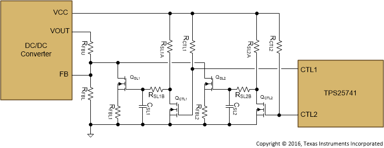
When transition slew control is required, the interaction of the slew mechanism and dc/dc converter loop response must be considered. A simple R-C filter between the device CTL pins and converter feedback node may lead to instability under some conditions. Figure 46 shows a method which manages the slew control without adding capacitance to the converter feedback node.
 Figure 46. Slew-Rate Control Example Number 1
When VOUT = 5 V, both CTL1 and CTL2 are in a high impedance state. When a 5 V to 12 V transition is requested, CTL2 goes low and turns off QCTL2. QSL2 gate starts to rise towards VCC at a rate determined by RSL2A + RSL2B and CSL2. QSL2 gate continues to rise, until QSL2 is fully enhanced placing RFBL2 in parallel with RFBL. In similar fashion when CTL1 goes low, QCTL1 turns off allowing RFBL1 to slew in parallel with RFBL2 and RFBL.
The slewing resistors and capacitor can be chosen using the following equations. VT is the VGS threshold voltage of QSL1 and QSL2. VREF is the feedback regulator reference voltage. Choose the slewing resistance in the 100 kΩ range to reduce the loading on the bias voltage source (VCC) and then calculate CSL. The falling transitions are shorter than the rising transitions in this topology.
Falling transitions:
- 20 V to 12 V

- 12 V to 5 V

Rising transitions:
- 5 V to 12 V

- 12 V to 20 V

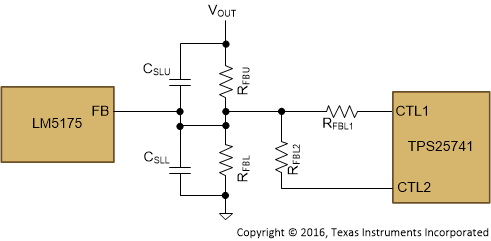
Some converter regulators can tolerate a balance of capacitance on the feedback node without affecting loop stability. The LM5175 has been tested using Figure 47 to combine VOUT slewing with a minimal amount of extra circuitry.
 Figure 47. Slew-Rate Control Example Number 2
When a higher voltage is requested from TPS25741, CTL1 or CTL2 goes low changing the sensed voltage at the FB pin. The LM5175 compensates by increasing VOUT. As VOUT increases, CSLU is charged at a rate proportional to RFBU. Three time constants yield a voltage change of approximately 95% and can be used to calculate the desired slew time. CSLU can be calculated using Equation 10 and Equation 11.


In order to minimize loop stability effects, a capacitor CSLL in parallel with RFBL is required. The ratio of CSLU/CSLL should be chosen to match the ratio of RFBL/RFBU. Choose CSLL according to Equation 12.

All slew rate control methods should be verified on the bench to ensure that the slew rate requirements are being met when the external VBUS capacitance is between 1 μF and 100 μF.