SLVSH93A October 2023 – March 2024 TPS25751
PRODUCTION DATA
- 1
- 1 Features
- 2 Applications
- 3 Description
- 4 Device Comparison Table
- 5 Pin Configuration and Functions
-
6 Specifications
- 6.1 Absolute Maximum Ratings
- 6.2 ESD Ratings
- 6.3 Recommended Operating Conditions
- 6.4 Recommended Capacitance
- 6.5 Thermal Information
- 6.6 Power Supply Characteristics
- 6.7 Power Consumption
- 6.8 PP_5V Power Switch Characteristics
- 6.9 PPHV Power Switch Characteristics - TPS25751D
- 6.10 PP_EXT Power Switch Characteristics - TPS25751S
- 6.11 Power Path Supervisory
- 6.12 CC Cable Detection Parameters
- 6.13 CC VCONN Parameters
- 6.14 CC PHY Parameters
- 6.15 Thermal Shutdown Characteristics
- 6.16 ADC Characteristics
- 6.17 Input/Output (I/O) Characteristics
- 6.18 BC1.2 Characteristics
- 6.19 I2C Requirements and Characteristics
- 6.20 Typical Characteristics
- 7 Parameter Measurement Information
-
8 Detailed Description
- 8.1 Overview
- 8.2 Functional Block Diagram
- 8.3
Feature Description
- 8.3.1 USB-PD Physical Layer
- 8.3.2 Power Management
- 8.3.3 Power Paths
- 8.3.4 Cable Plug and Orientation Detection
- 8.3.5 Overvoltage Protection (CC1, CC2)
- 8.3.6 Default Behavior Configuration (ADCIN1, ADCIN2)
- 8.3.7 ADC
- 8.3.8 BC 1.2 (USB_P, USB_N)
- 8.3.9 Digital Interfaces
- 8.3.10 Digital Core
- 8.3.11 I2C Interface
- 8.4 Device Functional Modes
- 8.5 Thermal Shutdown
-
9 Application and Implementation
- 9.1 Application Information
- 9.2 Typical Application
- 9.3 Power Supply Recommendations
- 9.4
Layout
- 9.4.1 TPS25751D - Layout
- 9.4.2 TPS25751S - Layout
- 10Device and Documentation Support
- 11Revision History
- 12Mechanical, Packaging, and Orderable Information
Package Options
Mechanical Data (Package|Pins)
Thermal pad, mechanical data (Package|Pins)
- RSM|32
Orderable Information
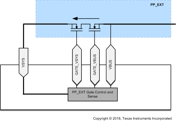
8.3.3.3 TPS25751S - External Sink Path Control PP_EXT
The TPS25751S has two N-ch gate drivers designed to control a sinking path from VBUS to VSYS. The charge pump for these gate drivers requires VBUS to be above VVBUS_UVLO. When a sink path is enabled, the circuitry includes a slew rate control loop to ensure that external switches do not turn on too quickly (SS). The TPS25751S senses the VSYS and VBUS voltages to control the gate voltages to enable or disable the external FETs.
The sink-path control includes overvoltage protection (OVP), and reverse current protection (RCP). Adding resistance in series with a GATE pin of the TPS25751S and the gate pin of the N-ch MOSFET slows down the turnoff time when OVP or RCP occurs. Any such resistance must be minimized, and not allowed to exceed 3 Ω.
 Figure 8-16 PP_EXT External
Sink Path Control
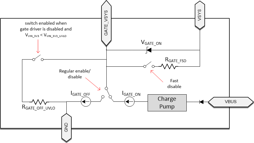
 Figure 8-17 Details of the VSYS Gate
Driver