SLVSH93A October   2023  – March 2024 TPS25751

PRODUCTION DATA  

  1.   1
  2. Features
  3. Applications
  4. Description
  5. Device Comparison Table
  6. Pin Configuration and Functions
  7. Specifications
    1. 6.1  Absolute Maximum Ratings
      1. 6.1.1 TPS25751D and TPS25751S - Absolute Maximum Ratings
      2. 6.1.2 TPS25751D - Absolute Maximum Ratings
      3. 6.1.3 TPS25751S - Absolute Maximum Ratings
    2. 6.2  ESD Ratings
    3. 6.3  Recommended Operating Conditions
      1. 6.3.1 TPS25751D - Recommended Operating Conditions
      2. 6.3.2 TPS25751S - Recommended Operating Conditions
    4. 6.4  Recommended Capacitance
    5. 6.5  Thermal Information
      1. 6.5.1 TPS25751D - Thermal Information
      2. 6.5.2 TPS25751S - Thermal Information
    6. 6.6  Power Supply Characteristics
    7. 6.7  Power Consumption
    8. 6.8  PP_5V Power Switch Characteristics
    9. 6.9  PPHV Power Switch Characteristics - TPS25751D
    10. 6.10 PP_EXT Power Switch Characteristics - TPS25751S
    11. 6.11 Power Path Supervisory
    12. 6.12 CC Cable Detection Parameters
    13. 6.13 CC VCONN Parameters
    14. 6.14 CC PHY Parameters
    15. 6.15 Thermal Shutdown Characteristics
    16. 6.16 ADC Characteristics
    17. 6.17 Input/Output (I/O) Characteristics
    18. 6.18 BC1.2 Characteristics
    19. 6.19 I2C Requirements and Characteristics
    20. 6.20 Typical Characteristics
  8. Parameter Measurement Information
  9. Detailed Description
    1. 8.1 Overview
    2. 8.2 Functional Block Diagram
    3. 8.3 Feature Description
      1. 8.3.1  USB-PD Physical Layer
        1. 8.3.1.1 USB-PD Encoding and Signaling
        2. 8.3.1.2 USB-PD Bi-Phase Marked Coding
        3. 8.3.1.3 USB-PD Transmit (TX) and Receive (Rx) Masks
        4. 8.3.1.4 USB-PD BMC Transmitter
        5. 8.3.1.5 USB-PD BMC Receiver
        6. 8.3.1.6 Squelch Receiver
      2. 8.3.2  Power Management
        1. 8.3.2.1 Power-On And Supervisory Functions
        2. 8.3.2.2 VBUS LDO
      3. 8.3.3  Power Paths
        1. 8.3.3.1 Internal Sourcing Power Paths
          1. 8.3.3.1.1 PP_5V Current Clamping
          2. 8.3.3.1.2 PP_5V Local Overtemperature Shut Down (OTSD)
          3. 8.3.3.1.3 PP_5V OVP
          4. 8.3.3.1.4 PP_5V UVLO
          5. 8.3.3.1.5 PP_5Vx Reverse Current Protection
          6. 8.3.3.1.6 PP_CABLE Current Clamp
          7. 8.3.3.1.7 PP_CABLE Local Overtemperature Shut Down (OTSD)
          8. 8.3.3.1.8 PP_CABLE UVLO
        2. 8.3.3.2 TPS25751D Internal Sink Path
          1. 8.3.3.2.1 Overvoltage Protection (OVP)
          2. 8.3.3.2.2 Reverse-Current Protection (RCP)
          3. 8.3.3.2.3 VBUS UVLO
          4. 8.3.3.2.4 Discharging VBUS to Safe Voltage
        3. 8.3.3.3 TPS25751S - External Sink Path Control PP_EXT
          1. 8.3.3.3.1 Overvoltage Protection (OVP)
            1. 8.3.3.3.1.1 Reverse-Current Protection (RCP)
            2. 8.3.3.3.1.2 VBUS UVLO
            3. 8.3.3.3.1.3 Discharging VBUS to Safe Voltage
      4. 8.3.4  Cable Plug and Orientation Detection
        1. 8.3.4.1 Configured as a Source
        2. 8.3.4.2 Configured as a Sink
        3. 8.3.4.3 Configured as a DRP
        4. 8.3.4.4 Dead Battery Advertisement
      5. 8.3.5  Overvoltage Protection (CC1, CC2)
      6. 8.3.6  Default Behavior Configuration (ADCIN1, ADCIN2)
      7. 8.3.7  ADC
      8. 8.3.8  BC 1.2 (USB_P, USB_N)
      9. 8.3.9  Digital Interfaces
        1. 8.3.9.1 General GPIO
        2. 8.3.9.2 I2C Interface
      10. 8.3.10 Digital Core
      11. 8.3.11 I2C Interface
        1. 8.3.11.1 I2C Interface Description
          1. 8.3.11.1.1 I2C Clock Stretching
          2. 8.3.11.1.2 I2C Address Setting
          3. 8.3.11.1.3 Unique Address Interface
    4. 8.4 Device Functional Modes
      1. 8.4.1 Pin Strapping to Configure Default Behavior
      2. 8.4.2 Power States
    5. 8.5 Thermal Shutdown
  10. Application and Implementation
    1. 9.1 Application Information
    2. 9.2 Typical Application
      1. 9.2.1 Design Requirements
        1. 9.2.1.1 Programmable Power Supply (PPS) - Design Requirements
        2. 9.2.1.2 Liquid Detection Design Requirements
        3. 9.2.1.3 BC1.2 Application Design Requirements
        4. 9.2.1.4 USB Data Support Design Requirements
      2. 9.2.2 Detailed Design Procedure
        1. 9.2.2.1 Programmable Power Supply (PPS)
        2. 9.2.2.2 Liquid Detection
          1. 9.2.2.2.1 Liquid Detection Operation
        3. 9.2.2.3 BC1.2 Application
        4. 9.2.2.4 USB Data Support
      3. 9.2.3 Application Curves
        1. 9.2.3.1 Programmable Power Supply (PPS) Application Curves
        2. 9.2.3.2 Liquid Detection Application Curves
        3. 9.2.3.3 BC1.2 Application Curves
        4. 9.2.3.4 USB Data Support Application Curves
    3. 9.3 Power Supply Recommendations
      1. 9.3.1 3.3-V Power
        1. 9.3.1.1 VIN_3V3 Input Switch
      2. 9.3.2 1.5-V Power
      3. 9.3.3 Recommended Supply Load Capacitance
    4. 9.4 Layout
      1. 9.4.1 TPS25751D - Layout
        1. 9.4.1.1 Layout Guidelines
          1. 9.4.1.1.1 Recommended Via Size
          2. 9.4.1.1.2 Minimum Trace Widths
        2. 9.4.1.2 Layout Example
          1. 9.4.1.2.1 TPS25751D Schematic Layout Example
          2. 9.4.1.2.2 TPS25751D Layout Example - PCB Plots
            1. 9.4.1.2.2.1 TPS25751D Component Placement
            2. 9.4.1.2.2.2 TPS25751D PP5V
            3. 9.4.1.2.2.3 TPS25751D PPHV
            4. 9.4.1.2.2.4 TPS25751D VBUS
            5. 9.4.1.2.2.5 TPS25751D I/O (I2C, ADCINs, GPIOs)
            6. 9.4.1.2.2.6 TPS25751D DRAIN
            7. 9.4.1.2.2.7 TPS25751D GND
      2. 9.4.2 TPS25751S - Layout
        1. 9.4.2.1 Layout Guidelines
          1. 9.4.2.1.1 Recommended Via Size
          2. 9.4.2.1.2 Minimum Trace Widths
        2. 9.4.2.2 Layout Example
          1. 9.4.2.2.1 TPS25751S Schematic Layout Example
          2. 9.4.2.2.2 TPS25751S Layout Example - PCB Plots
            1. 9.4.2.2.2.1 TPS25751S Component Placement
            2. 9.4.2.2.2.2 TPS25751S PP5V
            3. 9.4.2.2.2.3 TPS25751S PP_EXT
            4. 9.4.2.2.2.4 TPS25751S VBUS
            5. 9.4.2.2.2.5 TPS25751S I/O
            6. 9.4.2.2.2.6 TPS25751S PPEXT Gate Driver
            7. 9.4.2.2.2.7 TPS25751S GND
  11. 10Device and Documentation Support
    1. 10.1 Device Support
      1. 10.1.1 Third-Party Products Disclaimer
      2. 10.1.2 Firmware Warranty Disclaimer
    2. 10.2 Documentation Support
      1. 10.2.1 Related Documentation
    3. 10.3 Receiving Notification of Documentation Updates
    4. 10.4 Support Resources
    5. 10.5 Trademarks
    6. 10.6 Electrostatic Discharge Caution
    7. 10.7 Glossary
  12. 11Revision History
  13. 12Mechanical, Packaging, and Orderable Information

Package Options

Mechanical Data (Package|Pins)
Thermal pad, mechanical data (Package|Pins)
Orderable Information
Overvoltage Protection (OVP)

The application firmware enables the OVP and configures it based on the expected VBUS voltage. If the voltage on VBUS surpasses the configured threshold VOVP4VSYS = VOVP4RCP/rOVP, then GATE_VSYS is automatically disabled within tPPHV_FSD to protect the system. If the voltage on VBUS surpasses the configured threshold VOVP4RCP, then GATE_VBUS is automatically disabled within tPPHV_OVP. When VVBUS falls below VOVP4RCP - VOVP4RCPH, GATE_VBUS is automatically re-enabled within tPPHV_ON because the OVP condition has cleared. This action allows two sinking power paths to be enabled simultaneously and GATE_VBUS disables when necessary to ensure that VVBUS remains below VOVP4RCP.

While the TPS25751D is in BOOT mode in a dead-battery scenario (that is VIN_3V3 is low), it handles an OVP condition slightly differently. As long as the OVP condition is present, GATE_VBUS and GATE_VSYS are disabled. Once the OVP condition clears, both GATE_VBUS and GATE_VSYS are re-enabled. Because this is a dead-battery condition, the TPS25751D draws approximately IVIN_3V3, ActSnk from VBUS during this time to help discharge it.
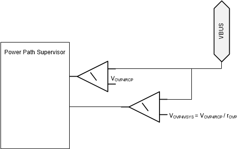
GUID-BE1DDAFC-00DF-4BC5-80E2-82898C9ED80E-low.gif Figure 8-18 Diagram for OVP Comparators