SLVSGL9B December 2022 – October 2024 TPS25762-Q1
PRODUCTION DATA
- 1
- 1 Features
- 2 Applications
- 3 Description
- 4 Device Comparison Table
- 5 Pin Configuration and Functions
-
6 Specifications
- 6.1 Absolute Maximum Ratings
- 6.2 ESD Ratings
- 6.3 Recommended Operating Conditions
- 6.4 Recommended Components
- 6.5 Thermal Information
- 6.6 Buck-Boost Regulator
- 6.7 CC Cable Detection Parameters
- 6.8 CC VCONN Parameters
- 6.9 CC PHY Parameters
- 6.10 Thermal Shutdown Characteristics
- 6.11 Oscillator Characteristics
- 6.12 ADC Characteristics
- 6.13 TVSP Parameters
- 6.14 Input/Output (I/O) Characteristics
- 6.15 BC1.2 Characteristics
- 6.16 I2C Requirements and Characteristics
- 6.17 Typical Characteristics
- 7 Parameter Measurement Information
-
8 Detailed Description
- 8.1 Overview
- 8.2 Functional Block Diagram
- 8.3
Feature Description
- 8.3.1 Device Power Management and Supervisory Circuitry
- 8.3.2 TVSP Device Configuration and ESD Protection
- 8.3.3
Buck-Boost Regulator
- 8.3.3.1 Buck-Boost Regulator Operation
- 8.3.3.2 Switching Frequency, Frequency Dither, Phase-Shift and Synchronization
- 8.3.3.3 VIN Supply and VIN Over-Voltage Protection
- 8.3.3.4 Feedback Paths and Error Amplifiers
- 8.3.3.5 Transconductors and Compensation
- 8.3.3.6 Output Voltage DAC, Soft-Start and Cable Droop Compensation
- 8.3.3.7 VBUS Overvoltage Protection
- 8.3.3.8 VBUS Undervoltage Protection
- 8.3.3.9 Current Sense Resistor (RSNS) and Current Limit Operation
- 8.3.3.10 Buck-Boost Peak Current Limits
- 8.3.4 USB-PD Physical Layer
- 8.3.5 VCONN
- 8.3.6 Cable Plug and Orientation Detection
- 8.3.7 ADC
- 8.3.8 BC 1.2, Legacy and Fast Charging Modes (Px_DP, Px_DM)
- 8.3.9 USB2.0 Low-Speed Endpoint
- 8.3.10 Digital Interfaces
- 8.3.11 I2C Interface
- 8.3.12 Digital Core
- 8.3.13 NTC Input
- 8.3.14 Thermal Sensors and Thermal Shutdown
- 8.4 Device Functional Modes
- 9 Application and Implementation
- 10Device and Documentation Support
- 11Revision History
- 12Mechanical, Packaging, and Orderable Information
Package Options
Refer to the PDF data sheet for device specific package drawings
Mechanical Data (Package|Pins)
- RQL|29
Thermal pad, mechanical data (Package|Pins)
Orderable Information
8.3.5 VCONN
Internal VCONN sourcing power paths are firmware configurable. Using only the internal LDO_5V supply, PortA is able to draw 20 mA continuously. If an external 5-V regulator is connected to the LDO_5V pin and the application GUI settings are enabled, PortA is able to draw 200 mA continuously. When disabled, blocking FETs in the PortA VCONN paths protect the LDO_5V rail from high-voltage and reverse current.
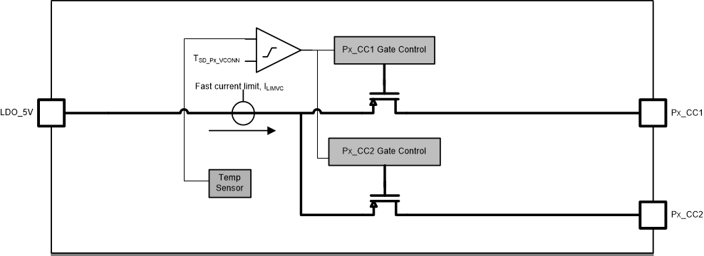
When VCONN power is enabled and provided, the internal VCONN power switches have a current limit of ILIMVC. If the VCONN load current exceeds ILIMVC, the current clamping circuit activates within tiOS_PP_CABLE and the switch behaves as a constant current source. Reverse current blocking is disabled when current is flowing to Px_CC1 or Px_CC2.
 Figure 8-26 VCONN Power Switches
When operating in current limit, the VCONN FET temperature rises. Local temperature sensors disable the Px_VCONN path in current limit when Tsensor > TSD_Px_VCONN within tPP_CABLE_off. The application firmware enters USB Type-C Error Recovery on the affected port.
LDO_5V must remain above its under voltage lock out threshold (VLDO_5V(UVLO_F)) for Px_VCONN operation. If the VLDO_5V(UVLO_F) threshold is reached, Px_VCONN paths are automatically disabled within tPP_CABLE_off.