SLVSGO0 October 2024 TPS25763-Q1
PRODUCTION DATA
- 1
- 1 Features
- 2 Applications
- 3 Description
- 4 Device Comparison Table
- 5 Pin Configuration and Functions
-
6 Specifications
- 6.1 Absolute Maximum Ratings
- 6.2 ESD Ratings
- 6.3 Recommended Operating Conditions
- 6.4 Recommended Components
- 6.5 Thermal Information
- 6.6 Buck-Boost Regulator
- 6.7 CC Cable Detection Parameters
- 6.8 CC VCONN Parameters
- 6.9 CC PHY Parameters
- 6.10 Thermal Shutdown Characteristics
- 6.11 Oscillator Characteristics
- 6.12 ADC Characteristics
- 6.13 TVSP Parameters
- 6.14 Input/Output (I/O) Characteristics
- 6.15 BC1.2 Characteristics
- 6.16 I2C Requirements and Characteristics
- 6.17 Typical Characteristics
- 7 Parameter Measurement Information
-
8 Detailed Description
- 8.1 Overview
- 8.2 Functional Block Diagram
- 8.3
Feature Description
- 8.3.1 Device Power Management and Supervisory Circuitry
- 8.3.2 TVSP Device Configuration and ESD Protection
- 8.3.3 External NFET and LSGD
- 8.3.4
Buck-Boost Regulator
- 8.3.4.1 Buck-Boost Regulator Operation
- 8.3.4.2 Switching Frequency, Frequency Dither, Phase-Shift and Synchronization
- 8.3.4.3 VIN Supply and VIN Over-Voltage Protection
- 8.3.4.4 Feedback Paths and Error Amplifiers
- 8.3.4.5 Transconductors and Compensation
- 8.3.4.6 Output Voltage DAC, Soft-Start and Cable Droop Compensation
- 8.3.4.7 VBUS Overvoltage Protection
- 8.3.4.8 VBUS Undervoltage Protection
- 8.3.4.9 Current Sense Resistor (RSNS) and Current Limit Operation
- 8.3.4.10 Buck-Boost Peak Current Limits
- 8.3.5 USB-PD Physical Layer
- 8.3.6 VCONN
- 8.3.7 Cable Plug and Orientation Detection
- 8.3.8 ADC
- 8.3.9 BC 1.2, Legacy and Fast Charging Modes (Px_DP, Px_DM)
- 8.3.10 DisplayPort Hot-Plug Detect (HPD)
- 8.3.11 USB2.0 Low-Speed Endpoint
- 8.3.12 Digital Interfaces
- 8.3.13 I2C Interface
- 8.3.14 Digital Core
- 8.3.15 NTC Input
- 8.3.16 Thermal Sensors and Thermal Shutdown
- 8.4 Device Functional Modes
- 9 Application and Implementation
- 10Device and Documentation Support
- 11Revision History
- 12Mechanical, Packaging, and Orderable Information
Package Options
Refer to the PDF data sheet for device specific package drawings
Mechanical Data (Package|Pins)
- RQL|29
Thermal pad, mechanical data (Package|Pins)
Orderable Information
8.3.4.2 Switching Frequency, Frequency Dither, Phase-Shift and Synchronization
The PWM oscillator frequency (fsw) is programmed by firmware using the application configuration GUI. The switching converter is intended for operation below the AM radio band (520 kHz - 1730 kHz). Three nominal fsw settings below are available: 300 kHz, 400 kHz and 450 kHz.
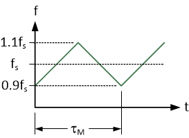
Frequency dithering can be enabled by firmware via the application GUI. When enabled, the nominal oscillator frequency is dithered by ±FSSS (approximately ±10%) using triangular waveform modulation (see Dithering using triangular waveform modulation). The dither period τM is the reciprocal of the dither modulation frequency FSSS_MOD. Two firmware selectable dither modulation frequencies FSSS_M are available: 10 and 25 kHz. Dithering spreads the spectral peaks generated by switching, thereby reducing the peak harmonic levels and easing EMI filter design.
 Figure 8-14 Dithering Using Triangular Waveform
Modulation
Figure 8-14 Dithering Using Triangular Waveform
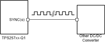
ModulationMultiple converters can be synchronized using the SYNC pin. This pin can be firmware-configured as either an output SYNC(o) or an input SYNC(i).
- SYNC(o): The switching clock is placed on the SYNC(o) pin. This
waveform has a duty cycle of approximately 50%. If frequency dithering is
configured by firmware, this signal also exhibits dithering. Four phase
settings are available by firmware configuration to shift the SYNC(o) output
relative to the internal switching clock by 0°, 90°, 120°, or 180°. SYNC(o)
is used to drive an external DC/DC converter clock with the switching
converter clock inside the TPS25763-Q1. When two dc/dc
converters operate out of phase, peak input current from the battery is
reduced and total input bulk capacitance requirements decrease.
Figure 8-15 SYNC(o) Phase Shift
 Figure 8-16 Using SYNC(o) to
drive external DC/DC Converter
 - SYNC(i): The internal clock is synchronized to the pulse train on the SYNC(i) pin. This feature is used to drive the TPS25763-Q1 with an external clock. The period of this clock must meet synchronization requirements in SYNC(i) frequency ranges or the TPS25763-Q1 instead uses its internal switching clock. If an external clock deviates outside of the acceptable frequency range and then returns to within the acceptable frequency range, the TPS25763-Q1 resumes operation from the external clock after counting 8 consecutive clocks meeting the criteria of Table 8-4. When SYNC(i) is configured, frequency dithering is disabled when operating from the internal clock following a failure of the external clock.
| fSW Firmware Setting | Allowed SYNC(i) Frequency Range | |
|---|---|---|
| MIN | MAX | |
| 300 kHz | 250 kHz | 353 kHz |
| 400 kHz | 334 kHz | 470 kHz |
| 450 kHz | 376 kHz | 530 kHz |