SBVS426B December 2022 – October 2024 TPS25772-Q1
PRODUCTION DATA
- 1
- 1 Features
- 2 Applications
- 3 Description
- 4 Device Comparison Table
- 5 Pin Configuration and Functions
-
6 Specifications
- 6.1 Absolute Maximum Ratings
- 6.2 ESD Ratings
- 6.3 Recommended Operating Conditions
- 6.4 Recommended Components
- 6.5 Thermal Information
- 6.6 Buck-Boost Regulator
- 6.7 CC Cable Detection Parameters
- 6.8 CC VCONN Parameters
- 6.9 CC PHY Parameters
- 6.10 Thermal Shutdown Characteristics
- 6.11 Oscillator Characteristics
- 6.12 ADC Characteristics
- 6.13 TVSP Parameters
- 6.14 Input/Output (I/O) Characteristics
- 6.15 BC1.2 Characteristics
- 6.16 I2C Requirements and Characteristics
- 6.17 Typical Characteristics
- 7 Parameter Measurement Information
-
8 Detailed Description
- 8.1 Overview
- 8.2 Functional Block Diagram
- 8.3
Feature Description
- 8.3.1 Device Power Management and Supervisory Circuitry
- 8.3.2 TVSP Device Configuration and ESD Protection
- 8.3.3
Buck-Boost Regulator
- 8.3.3.1 Buck-Boost Regulator Operation
- 8.3.3.2 Switching Frequency, Frequency Dither, Phase-Shift and Synchronization
- 8.3.3.3 VIN Supply and VIN Over-Voltage Protection
- 8.3.3.4 Feedback Paths and Error Amplifiers
- 8.3.3.5 Transconductors and Compensation
- 8.3.3.6 Output Voltage DAC, Soft-Start and Cable Droop Compensation
- 8.3.3.7 VBUS Overvoltage Protection
- 8.3.3.8 VBUS Undervoltage Protection
- 8.3.3.9 Current Sense Resistor (RSNS) and Current Limit Operation
- 8.3.3.10 Buck-Boost Peak Current Limits
- 8.3.4 USB-PD Physical Layer
- 8.3.5 VCONN
- 8.3.6 Cable Plug and Orientation Detection
- 8.3.7 ADC
- 8.3.8 BC 1.2, Legacy and Fast Charging Modes (Px_DP, Px_DM)
- 8.3.9 USB2.0 Low-Speed Endpoint
- 8.3.10 Digital Interfaces
- 8.3.11 I2C Interface
- 8.3.12 Digital Core
- 8.3.13 NTC Input
- 8.3.14 Thermal Sensors and Thermal Shutdown
- 8.4 Device Functional Modes
- 9 Application and Implementation
- 10Device and Documentation Support
- 11Revision History
- 12Mechanical, Packaging, and Orderable Information
Package Options
Refer to the PDF data sheet for device specific package drawings
Mechanical Data (Package|Pins)
- RQL|29
Thermal pad, mechanical data (Package|Pins)
Orderable Information
8.3.4.4 USB-PD BMC Transmitter
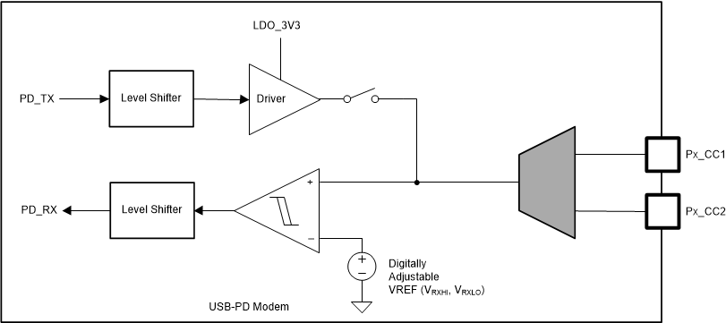
The TPS25772-Q1 transmits and receives USB-PD data over one of the Px_CCy pins for a given CC pin pair (one pair per USB Type-C port). The Px_CCy pins are also used to determine the cable orientation (see the Cable Plug and Orientation Detection section) and maintain cable/device attach detection. Thus, a DC bias exists on the Px_CCy pins. The transmitter driver overdrives the Px_CCy DC bias while transmitting, but returns to a Hi-Z state allowing the DC voltage to return to the Px_CCy pin when not transmitting. While either Px_CC1 or Px_CC2 may be used for transmitting and receiving, during a given connection only the one that mates with the CC pin of the plug is used; so there is no dynamic switching between Px_CC1 and Px_CC2. Figure 8-22 shows the USB-PD BMC TX and RX driver block diagram.
 Figure 8-22 USB-PD BMC TX/Rx
Block Diagram
Figure 8-22 USB-PD BMC TX/Rx
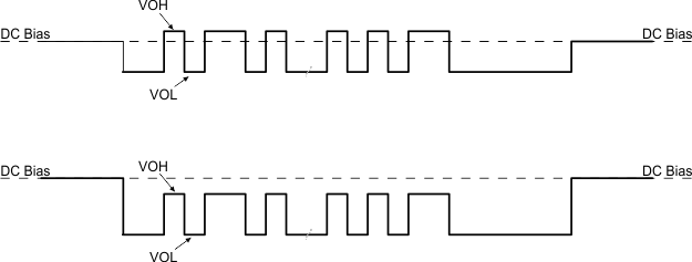
Block DiagramFigure 8-23 shows the transmission of the BMC data on top of the DC bias. Note, The DC bias can be anywhere between the minimum threshold for detecting a UFP attach and the maximum threshold for detecting a Sink attach to a Source resulting in a DC bias that can be above or below the VOH of the transmitter driver.
 Figure 8-23 TX Driver Transmission with DC Bias
The transmitter drives a digital signal onto the Px_CCy lines. The signal peak, VTXHI, is set to meet the TX masks defined in the USB-PD Specifications. Note that the TX mask is measured at the far-end of the cable.
When driving the line, the transmitter driver has an output impedance of ZDRIVER. ZDRIVER is determined by the driver resistance and the shunt capacitance of the source and is frequency dependent. ZDRIVER impacts the noise ingression in the cable.
 Figure 8-24 ZDRIVER Circuit