SLVSEZ5A July   2020  – December 2020 TPS25814

PRODUCTION DATA  

  1. Features
  2. Applications
  3. Description
  4. Revision History
  5. Pin Configuration and Functions
  6. Specifications
    1. 6.1  Absolute Maximum Ratings
    2. 6.2  ESD Ratings
    3. 6.3  Recommended Operating Conditions
    4. 6.4  Recommended Capacitance
    5. 6.5  Thermal Information
    6. 6.6  Power Supply Characteristics
    7. 6.7  Power Consumption
    8. 6.8  PP_5V Power Switch Characteristics
    9. 6.9  Power Path Supervisory
    10. 6.10 CC Cable Detection Parameters
    11. 6.11 CC VCONN Parameters
    12. 6.12 Thermal Shutdown Characteristics
    13. 6.13 Input/Output (I/O) Characteristics
    14. 6.14 BC1.2 Characteristics
    15. 6.15 I2C Requirements and Characteristics
    16. 6.16 Typical Characteristics
  7. Parameter Measurement Information
  8. Detailed Description
    1. 8.1 Overview
    2. 8.2 Functional Block Diagram
    3. 8.3 Feature Description
      1. 8.3.1 Power Paths
        1. 8.3.1.1 Internal Sourcing Power Paths
          1. 8.3.1.1.1 PP_5V Current Clamping
          2. 8.3.1.1.2 PP_5V Local Overtemperature Shut Down (OTSD)
          3. 8.3.1.1.3 PP_5V OVP
          4. 8.3.1.1.4 PP_5V UVLO
          5. 8.3.1.1.5 PP_5Vx Reverse Current Protection
          6. 8.3.1.1.6 PP_CABLE Current Clamp
          7. 8.3.1.1.7 PP_CABLE Local Overtemperature Shut Down (OTSD)
          8. 8.3.1.1.8 PP_CABLE UVLO
      2. 8.3.2 Cable Plug and Orientation Detection
        1. 8.3.2.1 Configured as a Source
      3. 8.3.3 Overvoltage Protection (CC1, CC2)
      4. 8.3.4 Default Behavior Configuration (ADCIN1, ADCIN2)
      5. 8.3.5 BC 1.2 (USB_P, USB_N)
      6. 8.3.6 Digital Interfaces
        1. 8.3.6.1 Fault Indicators ( FAULT )
        2. 8.3.6.2 Sink Attachment Indicator ( SINK )
        3. 8.3.6.3 Polarity Indicator ( POL )
        4. 8.3.6.4 Power Management ( CHG_HI)
        5. 8.3.6.5 Battery Charging Control (CTL)
        6. 8.3.6.6 Debug Accessory Detection ( DEBUG)
        7. 8.3.6.7 Disable the Port (EN)
        8. 8.3.6.8 I2C Interface
      7. 8.3.7 I2C Interface
        1. 8.3.7.1 I2C Interface Description
        2. 8.3.7.2 I2C Clock Stretching
        3. 8.3.7.3 I2C Address Setting
        4. 8.3.7.4 Unique Address Interface
    4. 8.4 Device Functional Modes
      1. 8.4.1 Pin Strapping to Configure Default Behavior
      2. 8.4.2 Power States
      3. 8.4.3 Schottky for Current Surge Protection
      4. 8.4.4 Thermal Shutdown
  9. Application and Implementation
    1. 9.1 Application Information
    2. 9.2 Typical Application
      1. 9.2.1 Type C DFP Port Implementation with Embedded Controller
        1. 9.2.1.1 Detailed Design Procedure
          1. 9.2.1.1.1 Type-C Connector VBUS Capacitors
          2. 9.2.1.1.2 VBUS Schottky and TVS Diodes
          3. 9.2.1.1.3 VBUS Snubber Circuit
        2. 9.2.1.2 Application Curves
  10. 10Power Supply Recommendations
    1. 10.1 3.3-V Power
      1. 10.1.1 VIN_3V3 Input Switch
    2. 10.2 1.5-V Power
    3. 10.3 Recommended Supply Load Capacitance
  11. 11Layout
    1. 11.1 Layout Guidelines
      1. 11.1.1 Top TPS25814 Placement and Bottom Component Placement and Layout
    2. 11.2 Layout Example
    3. 11.3 Component Placement
    4. 11.4 Routing and View Placement
  12. 12Device and Documentation Support
    1. 12.1 Device Support
      1. 12.1.1 Third-Party Products Disclaimer
    2. 12.2 Documentation Support
      1. 12.2.1 Related Documentation
    3. 12.3 Support Resources
    4. 12.4 Trademarks
    5. 12.5 Electrostatic Discharge Caution
    6. 12.6 Glossary
  13. 13Mechanical, Packaging, and Orderable Information

Package Options

Mechanical Data (Package|Pins)
Thermal pad, mechanical data (Package|Pins)
Orderable Information

Routing and View Placement

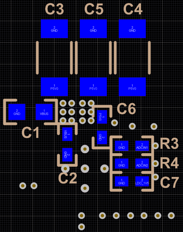
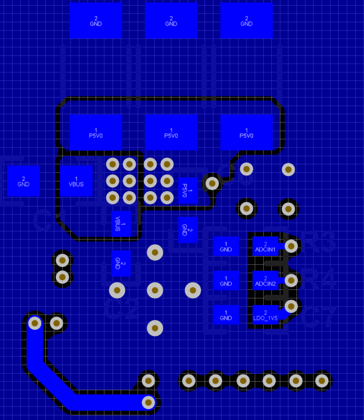
On the top side, create pours for PP5V and VBUS. Connect PP5V and VBUS from the top layer to the bottom layer using at least 6, 8-mil hole and 16-mil diameter vias. See Figure 11-6 for the recommended via sizing. The via placement and copper pours are highlighted in Figure 11-7.
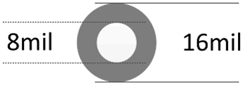
GUID-20200625-SS0I-G6MP-PRD2-TVJG2T4PBXTV-low.gif Figure 11-6 Recommended Minimum Via Sizing
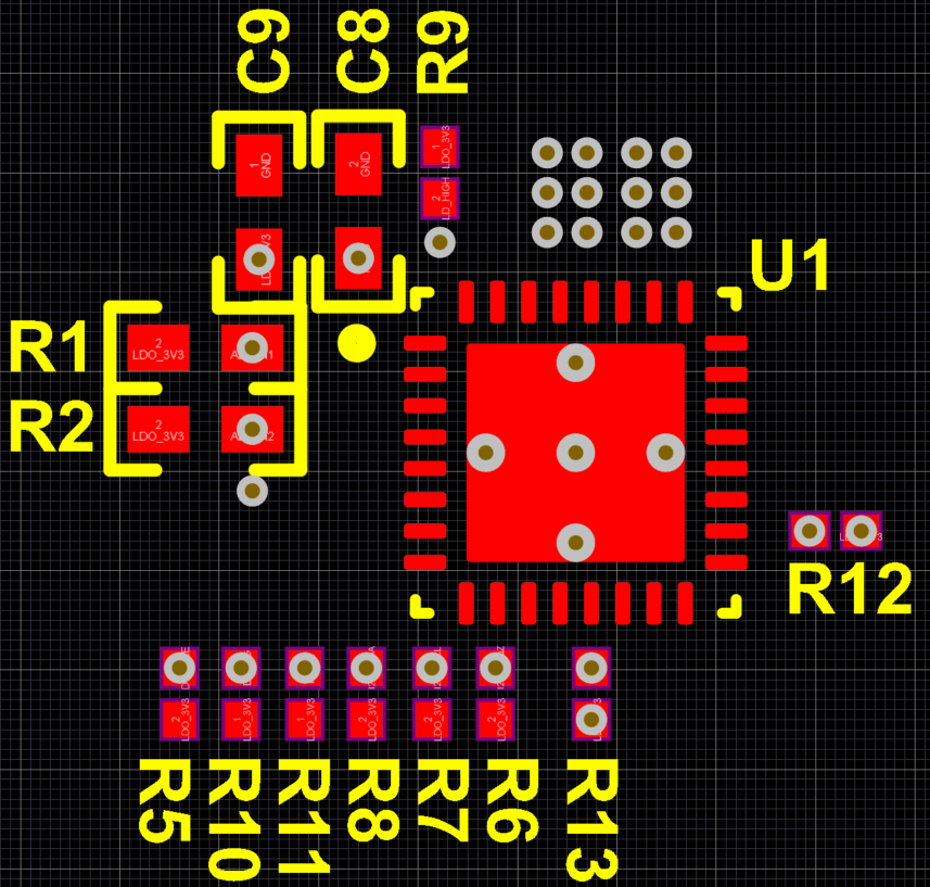
GUID-FFCF825C-B538-4E10-82E8-0D8D440A398A-low.png Figure 11-7 Via Placement - Top Layer
GUID-D15992A6-BCD4-4651-B03E-ED08CC1ADF9B-low.png Figure 11-8 Via Placement - Bottom Layer
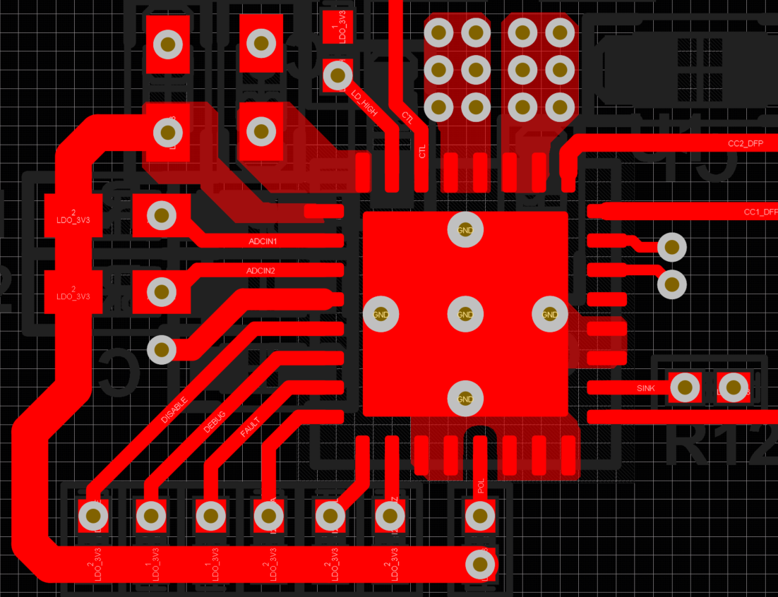
GUID-D8C5765D-F2C6-477C-A597-FF4AB1987D27-low.png Figure 11-9 Routing - Top Layer
GUID-7BBC1CDC-F948-4956-8DB9-A8F410DF11DF-low.png Figure 11-10 Routing - Bottom Layer