-
TPS2584x-Q1 Automotive USB Type-A BC1.2 5-V 3.5-A Output, 36-V Input Synchronous Buck With Cable Compensation SLVSEG3E September 2019 – March 2022 TPS25840-Q1 , TPS25842-Q1
PRODUCTION DATA
-
TPS2584x-Q1 Automotive USB Type-A BC1.2 5-V 3.5-A Output, 36-V Input Synchronous Buck With Cable Compensation
- 1 Features
- 2 Applications
- 3 Description
- 4 Revision History
- 5 Description (Continued)
- 6 Device Comparison Table
- 7 Pin Configuration and Functions
- 8 Specifications
- 9 Parameter Measurement Information
-
10Detailed Description
- 10.1 Overview
- 10.2 Functional Block Diagram
- 10.3
Feature Description
- 10.3.1 Buck Regulator
- 10.3.2 Enable/UVLO
- 10.3.3 Switching Frequency and Synchronization (RT/SYNC)
- 10.3.4 Spread-Spectrum Operation
- 10.3.5 VCC, VCC_UVLO
- 10.3.6 Minimum ON-time, Minimum OFF-time
- 10.3.7 Internal Compensation
- 10.3.8 Bootstrap Voltage (BOOT)
- 10.3.9 RSNS, RSET, RILIMIT and RIMON
- 10.3.10 Overcurrent and Short Circuit Protection
- 10.3.11 Overvoltage, IEC and Short-to-Battery Protection
- 10.3.12 Cable Compensation
- 10.3.13 USB Port Control
- 10.3.14 FAULT Response
- 10.3.15 USB Specification Overview
- 10.3.16 Device Power Pins (IN, CSN/OUT, and PGND)
- 10.3.17 Thermal Shutdown
- 10.4 Device Functional Modes
-
11Application and Implementation
- 11.1 Application Information
- 11.2
Typical Application
- 11.2.1 Design Requirements
- 11.2.2
Detailed Design Procedure
- 11.2.2.1 Output Voltage
- 11.2.2.2 Switching Frequency
- 11.2.2.3 Inductor Selection
- 11.2.2.4 Output Capacitor Selection
- 11.2.2.5 Input Capacitor Selection
- 11.2.2.6 Bootstrap Capacitor Selection
- 11.2.2.7 VCC Capacitor Selection
- 11.2.2.8 Enable and Under Voltage Lockout Set-Point
- 11.2.2.9 Current Limit Set-Point
- 11.2.2.10 Cable Compensation Set-Point
- 11.2.2.11 FAULT Resistor Selection
- 11.2.3 Application Curves
- 12Power Supply Recommendations
- 13Layout
- 14Device and Documentation Support
- 15Mechanical, Packaging, and Orderable Information
- IMPORTANT NOTICE
Package Options
Mechanical Data (Package|Pins)
- RHB|32
Thermal pad, mechanical data (Package|Pins)
- RHB|32
Orderable Information
TPS2584x-Q1 Automotive USB Type-A BC1.2 5-V 3.5-A Output, 36-V Input Synchronous Buck With Cable Compensation
1 Features
- AEC-Q100 qualified for automotive applications:
- Temperature grade 1: –40°C to +125°C, TA
- HBM ESD Classification level H2
- CDM ESD Classification level C5
- Functional Safety-Capable
- Synchronous Buck DC/DC regulator
- Input voltage range: 4.5 V to 36 V
- Output current: 3.5 A
- 5.1-V output voltage with ±1% accuracy
- Current mode control
- Adjustable frequency: 300 kHz to 2.2 MHz
- Frequency synchronization to external clock
- FPWM with spread-spectrum dithering
- Internal compensation for ease of use
- Compliant to USB-IF standards
- CDP/SDP mode per USB BC1.2
- Optimized for USB power and communication
- User-programmable USB current limit
- Cable droop compensation up to 1.5 V
- High bandwidth data switches on DP and DM
- Client mode for system update
- Integrated protection
- VBUS Short-to-VBAT protection
- DP_IN and DM_IN Short-to-VBAT
(TPS25840-Q1 only) - DP_IN and DM_IN Short-to-VBUS
- DP_IN, DM_IN IEC 61000-4-2 rated
- ±8-kV contact and ±15-kV air discharge
- Fault flag reports
- 32-pin QFN package with wettable flank
2 Applications
3 Description
The TPS2584x-Q1 is a USB Type-A BC1.2 charging solution that includes a synchronous DC/DC converter. With cable droop compensation, the Vbus voltage remains constant regardless of load current, ensuring connected portable devices charge at optimal current and voltage even under heavy loads.
The TPS2584x-Q1 includes high bandwidth analog switches for DP and DM pass-through.
The TPS25840-Q1 also integrates short-to-battery protection on VBUS, DM_IN and DP_IN pins. These pins can withstand voltage up to 18 V. TPS25842-Q1 does not support data line (Dx) short-to-VBAT protection.
| PART NUMBER | PACKAGE | BODY SIZE (NOM) |
|---|---|---|
TPS25840-Q1 | VQFN (32) | 5.00 mm x 5.00 mm |
TPS25842-Q1 | VQFN (32) | 5.00 mm x 5.00 mm |
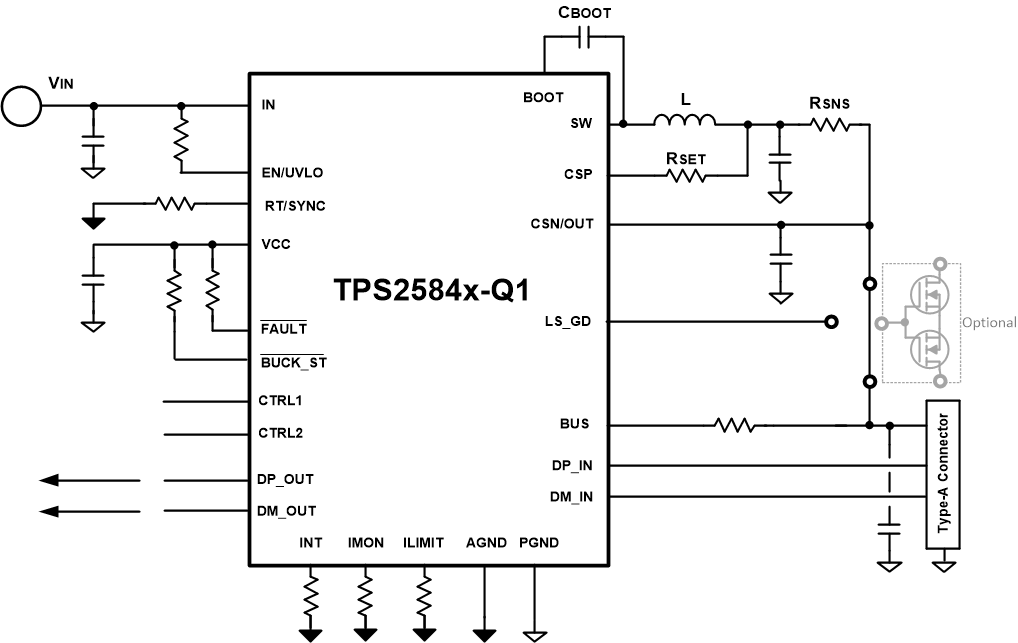
 Simplified Schematic TPS2584x-Q1
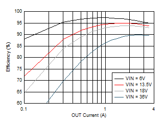
 Buck Efficiency vs Output
Current fsw = 400 kHz
Buck Efficiency vs Output
Current fsw = 400 kHz4 Revision History
Changes from Revision D (February 2022) to Revision E (March 2022)
- Added the thermal information for RHB0032AA packageGo
Changes from Revision C (December 2021) to Revision D (February 2022)
- Added RHB0032AA package to the data sheetGo
Changes from Revision B (August 2020) to Revision C (December 2021)
- Added additional description for Fault pin, for better signal quality under some sensitive application.Go
Changes from Revision A (May 2020) to Revision B (August 2020)
Changes from Revision * (September 2019) to Revision A (May 2020)
- Changed Section 13 description for clarityGo