SLVSEG3E September 2019 – March 2022 TPS25840-Q1 , TPS25842-Q1
PRODUCTION DATA
- 1 Features
- 2 Applications
- 3 Description
- 4 Revision History
- 5 Description (Continued)
- 6 Device Comparison Table
- 7 Pin Configuration and Functions
- 8 Specifications
- 9 Parameter Measurement Information
-
10Detailed Description
- 10.1 Overview
- 10.2 Functional Block Diagram
- 10.3
Feature Description
- 10.3.1 Buck Regulator
- 10.3.2 Enable/UVLO
- 10.3.3 Switching Frequency and Synchronization (RT/SYNC)
- 10.3.4 Spread-Spectrum Operation
- 10.3.5 VCC, VCC_UVLO
- 10.3.6 Minimum ON-time, Minimum OFF-time
- 10.3.7 Internal Compensation
- 10.3.8 Bootstrap Voltage (BOOT)
- 10.3.9 RSNS, RSET, RILIMIT and RIMON
- 10.3.10 Overcurrent and Short Circuit Protection
- 10.3.11 Overvoltage, IEC and Short-to-Battery Protection
- 10.3.12 Cable Compensation
- 10.3.13 USB Port Control
- 10.3.14 FAULT Response
- 10.3.15 USB Specification Overview
- 10.3.16 Device Power Pins (IN, CSN/OUT, and PGND)
- 10.3.17 Thermal Shutdown
- 10.4 Device Functional Modes
-
11Application and Implementation
- 11.1 Application Information
- 11.2
Typical Application
- 11.2.1 Design Requirements
- 11.2.2
Detailed Design Procedure
- 11.2.2.1 Output Voltage
- 11.2.2.2 Switching Frequency
- 11.2.2.3 Inductor Selection
- 11.2.2.4 Output Capacitor Selection
- 11.2.2.5 Input Capacitor Selection
- 11.2.2.6 Bootstrap Capacitor Selection
- 11.2.2.7 VCC Capacitor Selection
- 11.2.2.8 Enable and Under Voltage Lockout Set-Point
- 11.2.2.9 Current Limit Set-Point
- 11.2.2.10 Cable Compensation Set-Point
- 11.2.2.11 FAULT Resistor Selection
- 11.2.3 Application Curves
- 12Power Supply Recommendations
- 13Layout
- 14Device and Documentation Support
- 15Mechanical, Packaging, and Orderable Information
Package Options
Mechanical Data (Package|Pins)
- RHB|32
Thermal pad, mechanical data (Package|Pins)
- RHB|32
Orderable Information
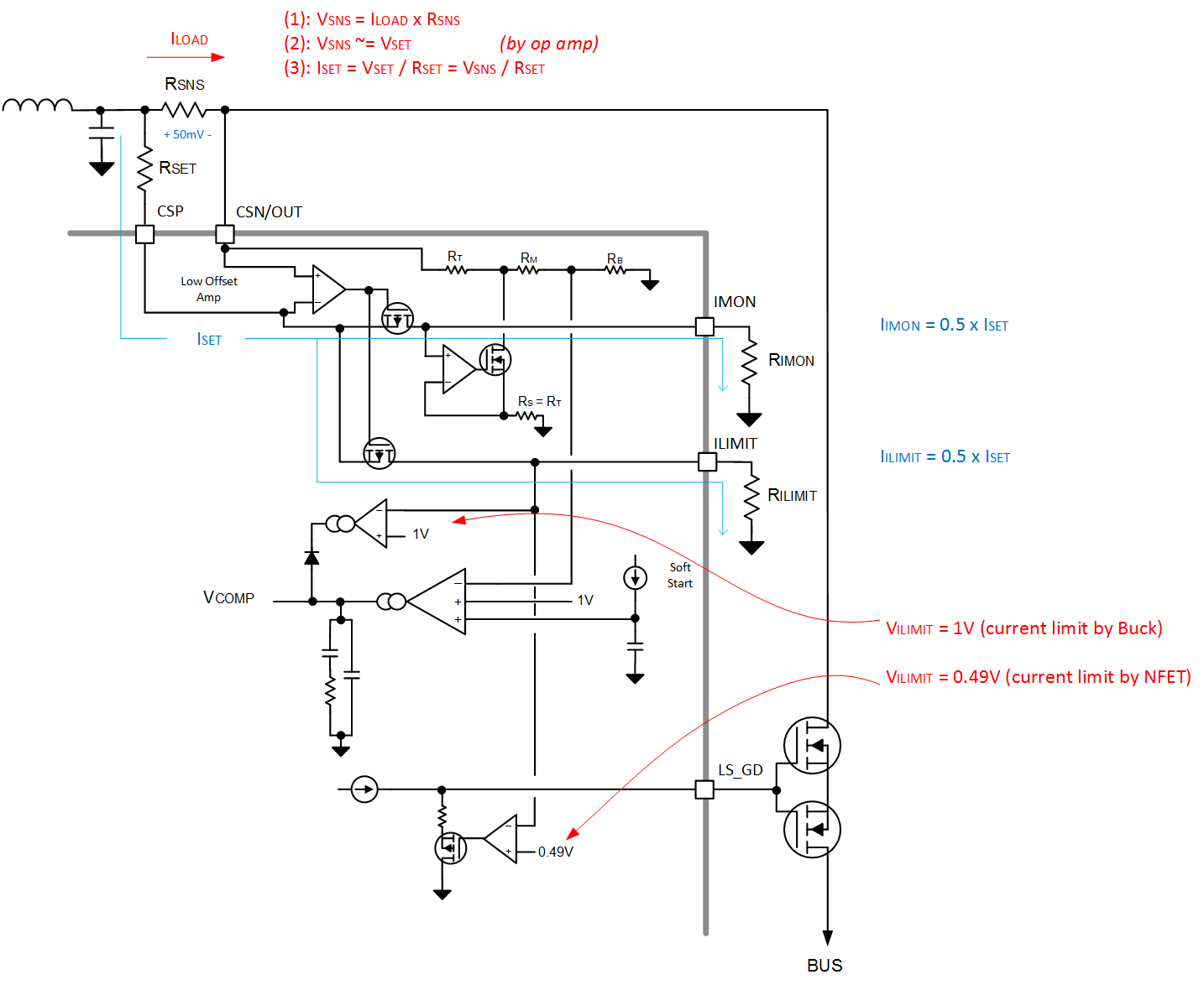
10.3.9 RSNS, RSET, RILIMIT and RIMON
The programmable current limit threshold and full-scale cable compensation voltage are determined by the values of the RSNS, RSET, RILIMIT and RIMON resistors. Refer to Figure 10-14.
- RSNS is the current sense resistor. The recommended voltage across RSNS under current limit must be approximately 50 mV as a compromise between accuracy and power dissipation. For example, if current limiting is desired for IOUT(MAX) ≥ 3.3 A, then RSNS = 0.05 V / 3.3 A = 0.01515 Ω. Choose a standard value of 15 mΩ.
- RSET determines the input current to the transconductance amplifier and current mirror. The amplifier balances the voltage to be equal to that across RSNS. Choose a RSET value to produce an ISET current between 75–180 µA at the desired IOUT(MAX). Considering 50 mV across RSET, a value of 300 Ω provides approximately 166 µA of ISET current to the amplifier and mirror circuit. Care must be taken to limit the ISET current below 200 µA to avoid saturating the internal amplifier circuit.
- RILIMIT in conjuction with the 0.5 × ISET current produces a voltage on the ILIMIT pin which is proportional to the load current flowing in RSNS. For details on setting the current limit, see Current Limit Sensing Using RILIMIT.
- RIMON in conjuction with the 0.5 × ISET current produces a voltage on the IMON pin which is proportional to the load current flowing in RSNS. For details on setting the current limit, see Cable Compensation.
 Figure 10-14 Current Limit and Cable Compensation Circuit