SLVSEG3E September 2019 – March 2022 TPS25840-Q1 , TPS25842-Q1
PRODUCTION DATA
- 1 Features
- 2 Applications
- 3 Description
- 4 Revision History
- 5 Description (Continued)
- 6 Device Comparison Table
- 7 Pin Configuration and Functions
- 8 Specifications
- 9 Parameter Measurement Information
-
10Detailed Description
- 10.1 Overview
- 10.2 Functional Block Diagram
- 10.3
Feature Description
- 10.3.1 Buck Regulator
- 10.3.2 Enable/UVLO
- 10.3.3 Switching Frequency and Synchronization (RT/SYNC)
- 10.3.4 Spread-Spectrum Operation
- 10.3.5 VCC, VCC_UVLO
- 10.3.6 Minimum ON-time, Minimum OFF-time
- 10.3.7 Internal Compensation
- 10.3.8 Bootstrap Voltage (BOOT)
- 10.3.9 RSNS, RSET, RILIMIT and RIMON
- 10.3.10 Overcurrent and Short Circuit Protection
- 10.3.11 Overvoltage, IEC and Short-to-Battery Protection
- 10.3.12 Cable Compensation
- 10.3.13 USB Port Control
- 10.3.14 FAULT Response
- 10.3.15 USB Specification Overview
- 10.3.16 Device Power Pins (IN, CSN/OUT, and PGND)
- 10.3.17 Thermal Shutdown
- 10.4 Device Functional Modes
-
11Application and Implementation
- 11.1 Application Information
- 11.2
Typical Application
- 11.2.1 Design Requirements
- 11.2.2
Detailed Design Procedure
- 11.2.2.1 Output Voltage
- 11.2.2.2 Switching Frequency
- 11.2.2.3 Inductor Selection
- 11.2.2.4 Output Capacitor Selection
- 11.2.2.5 Input Capacitor Selection
- 11.2.2.6 Bootstrap Capacitor Selection
- 11.2.2.7 VCC Capacitor Selection
- 11.2.2.8 Enable and Under Voltage Lockout Set-Point
- 11.2.2.9 Current Limit Set-Point
- 11.2.2.10 Cable Compensation Set-Point
- 11.2.2.11 FAULT Resistor Selection
- 11.2.3 Application Curves
- 12Power Supply Recommendations
- 13Layout
- 14Device and Documentation Support
- 15Mechanical, Packaging, and Orderable Information
Package Options
Mechanical Data (Package|Pins)
- RHB|32
Thermal pad, mechanical data (Package|Pins)
- RHB|32
Orderable Information
10.3.1 Buck Regulator
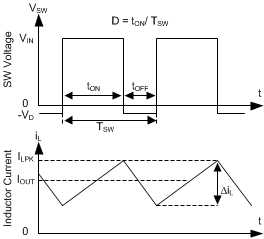
The following operating description of the TPS2584x-Q1 refers to the Functional Block Diagram and the waveforms in Figure 10-1. TPS2584x-Q1 is a step-down synchronous buck regulator with integrated high-side (HS) and low-side (LS) switches (synchronous rectifier). The TPS2584x-Q1 supplies a regulated output voltage by turning on the HS and LS NMOS switches with controlled duty cycle. During high-side switch ON time, the SW pin voltage swings up to approximately VIN, and the inductor current iL increase with linear slope (VIN – VOUT) / L. When the HS switch is turned off by the control logic, the LS switch is turned on after an anti-shoot-through dead time. Inductor current discharges through the LS switch with a slope of –VOUT / L. The control parameter of a buck converter is defined as Duty Cycle D = tON / TSW, where tON is the high-side switch ON time and TSW is the switching period. The regulator control loop maintains a constant output voltage by adjusting the duty cycle D. In an ideal buck converter, where losses are ignored, D is proportional to the output voltage and inversely proportional to the input voltage: D = VOUT / VIN.
 Figure 10-1 SW Node and Inductor Current Waveforms in Continuous Conduction Mode (CCM)
The TPS2584x-Q1 employs fixed frequency peak current mode control. A voltage feedback loop is used to get accurate DC voltage regulation by adjusting the peak current command based on voltage offset. The peak inductor current is sensed from the high-side switch and compared to the peak current threshold to control the ON time of the high-side switch. The voltage feedback loop is internally compensated, which allows for fewer external components, makes it easy to design, and provides stable operation with almost any combination of output capacitors. TPS2584x-Q1 operates in FPWM mode for low output voltage ripple, tight output voltage regulation, and constant switching frequency.