SLVSEG3E September 2019 – March 2022 TPS25840-Q1 , TPS25842-Q1
PRODUCTION DATA
- 1 Features
- 2 Applications
- 3 Description
- 4 Revision History
- 5 Description (Continued)
- 6 Device Comparison Table
- 7 Pin Configuration and Functions
- 8 Specifications
- 9 Parameter Measurement Information
-
10Detailed Description
- 10.1 Overview
- 10.2 Functional Block Diagram
- 10.3
Feature Description
- 10.3.1 Buck Regulator
- 10.3.2 Enable/UVLO
- 10.3.3 Switching Frequency and Synchronization (RT/SYNC)
- 10.3.4 Spread-Spectrum Operation
- 10.3.5 VCC, VCC_UVLO
- 10.3.6 Minimum ON-time, Minimum OFF-time
- 10.3.7 Internal Compensation
- 10.3.8 Bootstrap Voltage (BOOT)
- 10.3.9 RSNS, RSET, RILIMIT and RIMON
- 10.3.10 Overcurrent and Short Circuit Protection
- 10.3.11 Overvoltage, IEC and Short-to-Battery Protection
- 10.3.12 Cable Compensation
- 10.3.13 USB Port Control
- 10.3.14 FAULT Response
- 10.3.15 USB Specification Overview
- 10.3.16 Device Power Pins (IN, CSN/OUT, and PGND)
- 10.3.17 Thermal Shutdown
- 10.4 Device Functional Modes
-
11Application and Implementation
- 11.1 Application Information
- 11.2
Typical Application
- 11.2.1 Design Requirements
- 11.2.2
Detailed Design Procedure
- 11.2.2.1 Output Voltage
- 11.2.2.2 Switching Frequency
- 11.2.2.3 Inductor Selection
- 11.2.2.4 Output Capacitor Selection
- 11.2.2.5 Input Capacitor Selection
- 11.2.2.6 Bootstrap Capacitor Selection
- 11.2.2.7 VCC Capacitor Selection
- 11.2.2.8 Enable and Under Voltage Lockout Set-Point
- 11.2.2.9 Current Limit Set-Point
- 11.2.2.10 Cable Compensation Set-Point
- 11.2.2.11 FAULT Resistor Selection
- 11.2.3 Application Curves
- 12Power Supply Recommendations
- 13Layout
- 14Device and Documentation Support
- 15Mechanical, Packaging, and Orderable Information
Package Options
Mechanical Data (Package|Pins)
- RHB|32
Thermal pad, mechanical data (Package|Pins)
- RHB|32
Orderable Information
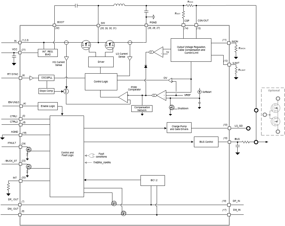
10.2 Functional Block Diagram
