SLVSEM3D May 2020 – September 2021 TPS25850-Q1 , TPS25851-Q1 , TPS25852-Q1
PRODUCTION DATA
- 1 Features
- 2 Applications
- 3 Description
- 4 Revision History
- 5 Description (continued)
- 6 Device Comparison Table
- 7 Pin Configuration and Functions
- 8 Specifications
- 9 Parameter Measurement Information
-
10Detailed Description
- 10.1 Overview
- 10.2 Functional Block Diagram
- 10.3
Feature Description
- 10.3.1 Power-Down or Undervoltage Lockout
- 10.3.2 Input Overvoltage Protection (OVP) - Continuously Monitored
- 10.3.3 Buck Converter
- 10.3.4 FREQ/SYNC
- 10.3.5 Bootstrap Voltage (BOOT)
- 10.3.6 Minimum ON-Time, Minimum OFF-Time
- 10.3.7 Internal Compensation
- 10.3.8 Selectable Output Voltage (VSET)
- 10.3.9 Current Limit and Short Circuit Protection
- 10.3.10 Cable Compensation
- 10.3.11 Thermal Management With Temperature Sensing (TS) and OTSD
- 10.3.12 Thermal Shutdown
- 10.3.13 USB Enable On/Off Control (TPS25852-Q1)
- 10.3.14 FAULT Indication (TPS25851-Q1 and TPS25852-Q1)
- 10.3.15 USB Specification Overview
- 10.3.16 USB Type-C® Basics
- 10.3.17 USB Port Operating Modes
- 10.4 Device Functional Modes
- 11Application and Implementation
- 12Power Supply Recommendations
- 13Layout
- 14Device and Documentation Support
- 15Mechanical, Packaging, and Orderable Information
Package Options
Mechanical Data (Package|Pins)
- RPQ|25
Thermal pad, mechanical data (Package|Pins)
Orderable Information
10.3.10 Cable Compensation
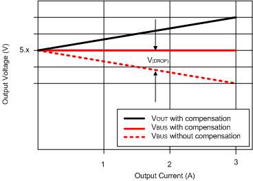
When a load draws current through a long or thin wire, there is an IR drop that reduces the voltage delivered to the load. In the vehicle from the voltage regulator output VOUT to VBUS (input voltage of portable device), the total resistance of PCB trace, connector, and cable resistances causes an IR drop at the portable device input, so the charging current of most portable devices is less than their expected maximum charging current. The voltage drop is shown in Figure 10-14.
 Figure 10-14 Voltage Drop
To handle this case, the TPS2585x-Q1 has a built-in cable compensation function where the droop compensation linearly increases the voltage at the SENSE pin of the TPS2585x-Q1 as load current increases, to maintain a fairly constant output voltage at the load-side voltage.
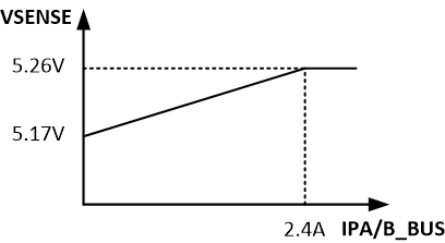
The TPS2585x-Q1 internal comparator compares the current-sense output voltage of the two current-limit switches and uses the larger current-sense output voltage to compensate for the line drop voltage. The cable compensation amplitude increases linearly as the load current increases. The cable compensation also has an upper limitation. The cable compensation at output currents greater than 2.4 A is 90 mV and is shown in Figure 10-15. Note the cable compensation only works when you short the VSET to GND. For the other VSET configuration, the cable compensation is not available.
 Figure 10-15 Dual Ports Cable
Compensation