SLVSFP1 August 2021 TPS25868-Q1 , TPS25869-Q1
PRODUCTION DATA
- 1 Features
- 2 Applications
- 3 Description
- 4 Revision History
- 5 Description (continued)
- 6 Device Comparison Table
- 7 Pin Configuration and Functions
- 8 Specifications
- 9 Parameter Measurement Information
-
10Detailed Description
- 10.1 Overview
- 10.2 Functional Block Diagram
- 10.3
Feature Description
- 10.3.1 Power-Down or Undervoltage Lockout
- 10.3.2 Input Overvoltage Protection (OVP) - Continuously Monitored
- 10.3.3 Buck Converter
- 10.3.4 FREQ/SYNC
- 10.3.5 Bootstrap Voltage (BOOT)
- 10.3.6 Minimum ON-Time, Minimum OFF-Time
- 10.3.7 Internal Compensation
- 10.3.8 Selectable Output Voltage (VSET)
- 10.3.9 Current Limit and Short Circuit Protection
- 10.3.10 Cable Compensation
- 10.3.11 Thermal Management with Temperature Sensing (TS) and OTSD
- 10.3.12 Thermal Shutdown
- 10.3.13 USB Enable On/Off Control (TPS25869-Q1)
- 10.3.14 FAULT Indication
- 10.3.15 USB Specification Overview
- 10.3.16 USB Type-C® Basics
- 10.3.17 USB Port Operating Modes
- 10.4 Device Functional Modes
-
11Application and Implementation
- 11.1 Application Information
- 11.2
Typical Applications
- 11.2.1 Design Requirements
- 11.2.2
Detailed Design Procedure
- 11.2.2.1 Output Voltage Setting
- 11.2.2.2 Switching Frequency
- 11.2.2.3 Inductor Selection
- 11.2.2.4 Output Capacitor Selection
- 11.2.2.5 Input Capacitor Selection
- 11.2.2.6 Bootstrap Capacitor Selection
- 11.2.2.7 Undervoltage Lockout Set-Point
- 11.2.2.8 Cable Compensation Set-Point
- 11.2.2.9 FAULT Resistor Selection
- 11.2.3 Application Curves
- 12Power Supply Recommendations
- 13Layout
- 14Device and Documentation Support
- 15Mechanical, Packaging, and Orderable Information
Package Options
Mechanical Data (Package|Pins)
- RPQ|25
Thermal pad, mechanical data (Package|Pins)
Orderable Information
10.3.4 FREQ/SYNC
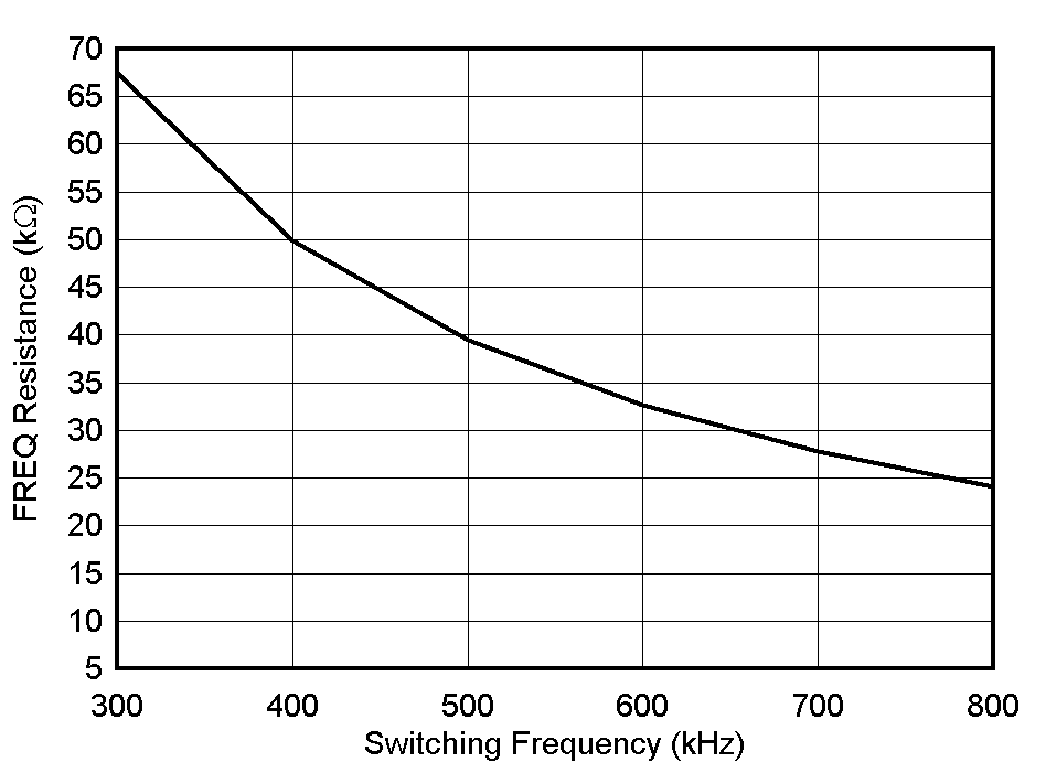
The switching frequency of the TPS2586x-Q1 can be programmed by the resistor RFREQ from the FREQ/SYNC pin and AGND pin. To determine the FREQ resistance, for a given switching frequency, use Equation 4:

 Figure 10-3 FREQ Set Resistor vs Switching
Frequency
Figure 10-3 FREQ Set Resistor vs Switching
FrequencyThe normal method of setting the buck regulator switching frequency is by selecting an appropriate value FREQ resistor as shown in Table 10-1.
| FREQ (KΩ) | SWITCHING FREQUENCY (KHz) |
|---|---|
| 80.6 | 253 |
| 49.9 | 400 |
The FREQ/SYNC pin can be used to synchronize the internal oscillator to an external clock. The internal oscillator can be synchronized by AC coupling a positive edge into the FREQ/SYNC pin. When using a low impedance signal source, the frequency setting resistor FREQ is connected in parallel with an AC coupling capacitor, CCOUP, to a termination resistor, RTERM (for example, 50 Ω). The two resistors in series provide the default frequency setting resistance when the signal source is turned off. A 10-pF ceramic capacitor can be used for CCOUP. The AC coupled peak-to-peak voltage at the FREQ/SYNC pin must exceed the SYNC amplitude threshold of 1.2 V (typical) to trip the internal synchronization pulse detector, and the minimum SYNC clock HIGH and LOW time must be longer than 100 ns (typical). A 2.5 V or higher amplitude pulse signal coupled through a 1-nF capacitor, CSYNC, is a good starting point. Figure 10-4 shows the device synchronized to an external system clock. The external clock must be off before start-up to allow proper start-up sequencing.
 Figure 10-4 Synchronize to External Clock
The TPS2586x-Q1 switching action can be synchronized to an external clock from 200 KHz to 800 KHz.