SLVSFP1 August 2021 TPS25868-Q1 , TPS25869-Q1
PRODUCTION DATA
- 1 Features
- 2 Applications
- 3 Description
- 4 Revision History
- 5 Description (continued)
- 6 Device Comparison Table
- 7 Pin Configuration and Functions
- 8 Specifications
- 9 Parameter Measurement Information
-
10Detailed Description
- 10.1 Overview
- 10.2 Functional Block Diagram
- 10.3
Feature Description
- 10.3.1 Power-Down or Undervoltage Lockout
- 10.3.2 Input Overvoltage Protection (OVP) - Continuously Monitored
- 10.3.3 Buck Converter
- 10.3.4 FREQ/SYNC
- 10.3.5 Bootstrap Voltage (BOOT)
- 10.3.6 Minimum ON-Time, Minimum OFF-Time
- 10.3.7 Internal Compensation
- 10.3.8 Selectable Output Voltage (VSET)
- 10.3.9 Current Limit and Short Circuit Protection
- 10.3.10 Cable Compensation
- 10.3.11 Thermal Management with Temperature Sensing (TS) and OTSD
- 10.3.12 Thermal Shutdown
- 10.3.13 USB Enable On/Off Control (TPS25869-Q1)
- 10.3.14 FAULT Indication
- 10.3.15 USB Specification Overview
- 10.3.16 USB Type-C® Basics
- 10.3.17 USB Port Operating Modes
- 10.4 Device Functional Modes
-
11Application and Implementation
- 11.1 Application Information
- 11.2
Typical Applications
- 11.2.1 Design Requirements
- 11.2.2
Detailed Design Procedure
- 11.2.2.1 Output Voltage Setting
- 11.2.2.2 Switching Frequency
- 11.2.2.3 Inductor Selection
- 11.2.2.4 Output Capacitor Selection
- 11.2.2.5 Input Capacitor Selection
- 11.2.2.6 Bootstrap Capacitor Selection
- 11.2.2.7 Undervoltage Lockout Set-Point
- 11.2.2.8 Cable Compensation Set-Point
- 11.2.2.9 FAULT Resistor Selection
- 11.2.3 Application Curves
- 12Power Supply Recommendations
- 13Layout
- 14Device and Documentation Support
- 15Mechanical, Packaging, and Orderable Information
Package Options
Mechanical Data (Package|Pins)
- RPQ|25
Thermal pad, mechanical data (Package|Pins)
Orderable Information
10.3.16.2 Detecting a Connection
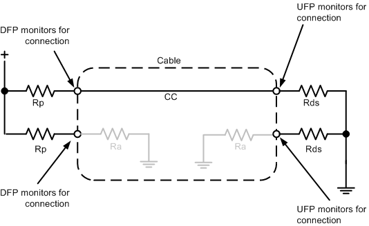
DFPs and DRPs fulfill the role of detecting a valid connection over USB Type-C. Figure 10-14 shows a DFP-to-UFP connection made with a Type-C cable. As shown in Figure 10-14, the detection concept is based on being able to detect terminations in the product that have been attached. A pull-up and pull-down termination model is used. A pull-up termination can be replaced by a current source.
- In the DFP-UFP connection, the DFP monitors both CC pins for a voltage lower than the unterminated voltage.
- An UFP advertises Rd on both its CC pins (CC1 and CC2).
- A powered cable advertises Ra on only one of the CC pins of the plug. Ra is used to inform the source to apply VCONN.
- An analog audio device advertises Ra on both CC pins of the plug, which identifies it as an analog audio device. VCONN is not applied on either CC pin in this case.
 Figure 10-14 DFP-UFP
Connection
Figure 10-14 DFP-UFP
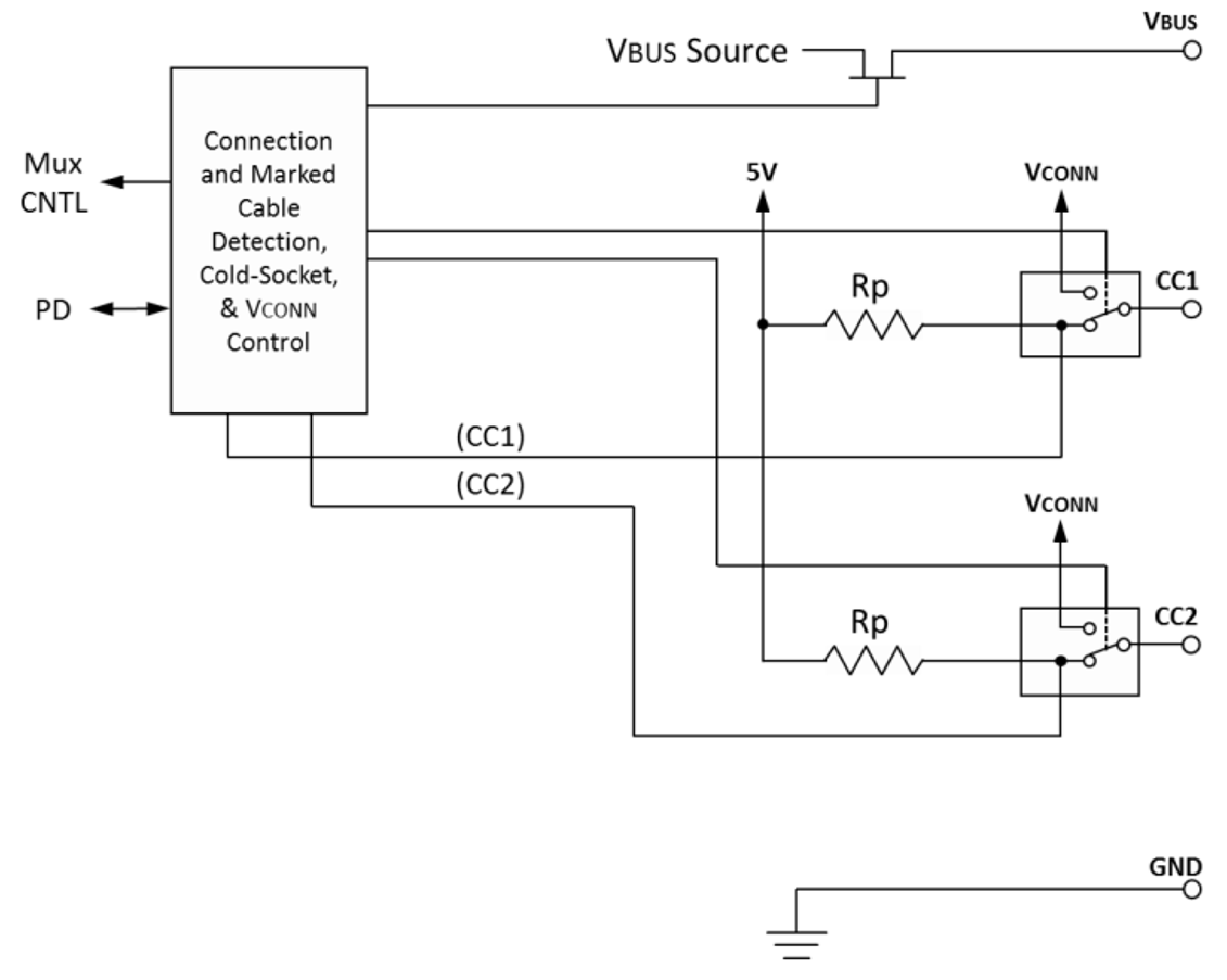
ConnectionFor USB Type-C solutions, two pins (CC1, CC2) on the connector are used to establish and manage the source-to-sink connection. The general concept for setting up a valid connection between a source and a sink is based on being able to detect terminations residing in the product being attached. To aid in defining the functional behavior of CC, a pull-up (Rp) and pull-down (Rd 5.1 kΩ) termination model is used based on a pull-up resistor and pull-down resistor.
Initially, a source exposes independent Rp terminations on its CC1 and CC2 pins, and a sink exposes independent Rd terminations on its CC1 and CC2 pins. The source-to-sink combination of this circuit configuration represents a valid connection. To detect this, the source monitors CC1 and CC2 for a voltage lower than its unterminated voltage. The choice of Rp is a function of the pull-up termination voltage and the detection circuit of the source. This indicates that either a sink, a powered cable, or a sink connected by a powered cable has been attached. Prior to the application of VCONN, a powered cable exposes Ra (typically 1 kΩ) on its VCONN pin. Ra represents the load on VCONN plus any resistive elements to ground. In some cable plugs, this might be a pure resistance, and in others, it can simply be the load. The CC pin functional block is shown in Figure 10-15.
 Figure 10-15 Source Functional Model for
CC1 and CC2 (From Type-C Specification)
Figure 10-15 Source Functional Model for
CC1 and CC2 (From Type-C Specification)The source must be able to differentiate between the presence of Rd and Ra to know whether there is a sink attached and where to apply VCONN. The source is not required to source VCONN unless Ra is detected. Two special termination combinations on the CC pins as seen by a source are defined for directly attached accessory modes: Ra/Ra for audio adapter accessory mode and Rd/Rd for debug accessory mode.