SLVSCU8E August 2015 – November 2017
PRODUCTION DATA.
- 1 Features
- 2 Applications
- 3 Description
- 4 Revision History
- 5 Pin Configuration and Functions
- 6 Specifications
- 7 Detailed Description
-
8 Application and Implementation
- 8.1 Application Information
- 8.2
Typical Application
- 8.2.1
Simple 2.1-A eFuse Protection for Set Top Boxes
- 8.2.1.1 Design Requirements
- 8.2.1.2 Detailed Design Procedure
- 8.2.1.3 Application Curves
- 8.2.2 Controlled Power Down using TPS25927x
- 8.2.1
Simple 2.1-A eFuse Protection for Set Top Boxes
- 9 Power Supply Recommendations
- 10Layout
- 11Device and Documentation Support
- 12Mechanical, Packaging, and Orderable Information
Package Options
Mechanical Data (Package|Pins)
- DRC|10
Thermal pad, mechanical data (Package|Pins)
- DRC|10
Orderable Information
8 Application and Implementation
NOTE
Information in the following applications sections is not part of the TI component specification, and TI does not warrant its accuracy or completeness. TI’s customers are responsible for determining suitability of components for their purposes. Customers should validate and test their design implementation to confirm system functionality.
8.1 Application Information
The TPA25927x is a smart eFuse. It is typically used for Hot-Swap and Power rail protection applications. It operates from 4.5 V to 18 V with programmable current limit and undervoltage protection. The device aids in controlling the in-rush current and provides precise current limiting during overload conditions for systems such as Set-Top-Box, DTVs, Gaming Consoles, SSDs/HDDs and Smart Meters. The device also provides robust protection for multiple faults on the sub-system rail.
The following design procedure can be used to select component values for the device. Alternatively, the WEBENCH® software may be used to generate a complete design. The WEBENCH® software uses an iterative design procedure and accesses a comprehensive database of components when generating a design. Additionally, a spreadsheet design tool TPS2592xx Design Calculator (SLUC570) is available on web folder. This section presents a simplified discussion of the design process.
8.2 Typical Application
8.2.1 Simple 2.1-A eFuse Protection for Set Top Boxes
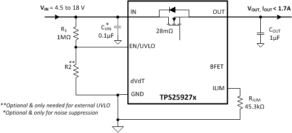 Figure 37. Typical Application Schematic: Simple e-Fuse for STBs
8.2.1.1 Design Requirements
Table 3 shows the design parameters for this application.
Table 3. Design Parameters
| DESIGN PARAMETER | EXAMPLE VALUE |
|---|---|
| Input voltage range, VIN | 12 V |
| Undervoltage lockout set point, V(UV) | Default: VUVR = 4.3 V |
| Load at start-up, RL(SU) | 8 Ω |
| Current limit, IOL = IILIM | 2.1 A |
| Load capacitance, COUT | 1 µF |
| Maximum ambient temperature, TA | 85°C |
8.2.1.2 Detailed Design Procedure
The following design procedure can be used to select component values for the TPS25927x.
8.2.1.2.1 Step by Step Design Procedure
This design procedure below seeks to control the junction temperature of device under both static and transient conditions by proper selection of output ramp-up time and associated support components. The designer can adjust this procedure to fit the application and design criteria.
8.2.1.2.2 Programming the Current-Limit Threshold: RILIM Selection
The RILIM resistor at the ILIM pin sets the over load current limit, this can be set using Equation 4:

For IOL = IILIM = 2.1 A, from Equation 4, RILIM = 45.3 kΩ, choose closest standard value resistor with 1% tolerance.
8.2.1.2.3 Undervoltage Lockout Set Point
The undervoltage lockout (UVLO) trip point is adjusted using the external voltage divider network of R1 and R2 as connected between IN, EN/UVLO and GND pins of the device. The values required for setting the undervoltage are calculated solving Equation 5:

Where VENR = 1.4 V is enable voltage rising threshold.
Since R1 and R2 leak the current from input supply (VIN), these resistors must be selected based on the acceptable leakage current from input power supply (VIN). The current drawn by R1 and R2 from the power supply {IR12 = VIN/(R1 + R2)}.
However, leakage currents due to external active components connected to the resistor string can add error to these calculations. So, the resistor string current, IR12 must be chosen to be 20x greater than the leakage current expected.
For default UVLO of VUVR = 4.3 V, select R2 = OPEN, and R1 = 1 MΩ. Since EN/UVLO pin is rated only to 7 V, it cannot be connected directly to VIN = 12 V. It has to be connected through R1 = 1 MΩ only, so that the pull-up current for EN/UVLO pin is limited to < 20 µA.
The power failure threshold is detected on the falling edge of supply. This threshold voltage is 4% lower than the rising threshold, VUVR. This is calculated using Equation 6:
Where VUVR is 4.3 V, Power fail threshold set is : 4.1 V.
8.2.1.2.4 Setting Output Voltage Ramp Time (TdVdT)
For a successful design, the junction temperature of device must be kept below the absolute-maximum rating during both dynamic (start-up) and steady state conditions. Dynamic power stresses often are an order of magnitude greater than the static stresses, so it is important to determine the right start-up time and in-rush current limit required with system capacitance to avoid thermal shutdown during start-up with and without load.
The ramp-up capacitor CdVdT needed is calculated considering the two possible cases:
8.2.1.2.4.1 Case 1: Start-Up without Load: Only Output Capacitance COUT Draws Current During Start-Up
During start-up, as the output capacitor charges, the voltage difference as well as the power dissipated across the internal FET decreases. The average power dissipated in the device during start-up is calculated using Equation 8.
For TPS25927x, the inrush current is determined using Equation 7:

Power dissipation during start-up is given by Equation 8:

Equation 8 assumes that load does not draw any current until the output voltage has reached its final value.
8.2.1.2.4.2 Case 2: Start-Up with Load: Output Capacitance COUT and Load Draws Current During Start-Up
When load draws current during the turnon sequence, there is additional power dissipated. Considering a resistive load during start-up (RL(SU)), load current ramps up proportionally with increase in output voltage during TdVdT time. The average power dissipation in the internal FET during charging time due to resistive load is given by Equation 9:

Total power dissipated in the device during startup is given by Equation 10:

Total current during start-up is given by Equation 11:

If I(STARTUP) > IOL, the device limits the current to IOL and the current limited charging time is determined by Equation 12:

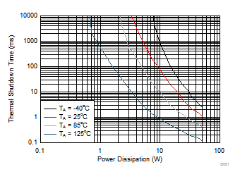
The power dissipation, with and without load, for selected start-up time must not exceed the shutdown limits as shown in Figure 38.
For the design example under discussion, select ramp-up capacitor CdVdT = OPEN. Then, using Equation 2 we get Equation 13:

The inrush current drawn by the load capacitance (COUT) during ramp-up using Equation 7 is given by Equation 14:

The inrush power dissipation is calculated, using Equation 8 as shown in Equation 15:

For 90 mW of power loss, the thermal shut down time of the device must not be less than the ramp-up time TdVdT to avoid the false trip at maximum operating temperature. From thermal shutdown limit graph Figure 38 at TA = 85°C, for 90 mW of power, the shutdown time is infinite. So it is safe to use 0.79 ms as start-up time without any load on output.
Considering the start-up with load 8 Ω, the additional power dissipation, when load is present during start-up is calculated, using Equation 9 we get Equation 16:

The total device power dissipation during start-up is given by Equation 17:

From thermal shutdown limit graph at TA = 85°C, the thermal shutdown time for 3.09 W is more than 100 ms. So it is well within acceptable limits to use no external capacitor (CdV/dT) with start-up load of 8 Ω.
If, due to large COUT, there is a need to decrease the power loss during start-up, it can be done with increase of CdVdT capacitor.
8.2.1.2.5 Support Component Selection—CVIN
CVIN is a bypass capacitor to help control transient voltages, unit emissions, and local supply noise. Where acceptable, a value in the range of 0.001 μF to 0.1 μF is recommended for CVIN.
8.2.2 Controlled Power Down using TPS25927x
When the device is disabled, the output voltage is left floating and power down profile is entirely dictated by the load. In some applications, this can lead to undesired activity as the load is not powered down to a defined state. Controlled output discharge can ensure the load is turned off completely and not in an undefined operational state. The BFET pin in TPS25927x family of eFuses facilitates Quick Output Discharge (QOD) function as illustrated in Figure 41 . When the device is/gets disabled, the BFET pin pulls low which enables the external P-MOSFET Q1 for discharge feature to function. The output voltage discharge rate is dictated by the output capacitor COUT, the discharge resistance RDCHG and the load.
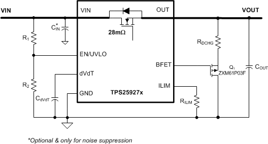 Figure 41. Circuit Implementation with Quick Output Discharge Function
