SLVSCU2 December 2014 TPS2592BA , TPS2592BL
PRODUCTION DATA.
- 1 Features
- 2 Applications
- 3 Description
- 4 Application Schematic
- 5 Revision History
- 6 Device Comparison Table
- 7 Pin Configuration and Functions
- 8 Specifications
- 9 Detailed Description
-
10Application and Implementation
- 10.1 Application Information
- 10.2
Typical Applications
- 10.2.1
Simple 3.7-A eFuse Protection for Set Top Boxes
- 10.2.1.1 Design Requirements
- 10.2.1.2 Detailed Design Procedure
- 10.2.1.3 Support Component Selection - CVIN
- 10.2.1.4 Application Curves
- 10.2.2 Inrush and Reverse Current Protection for Hold-Up Capacitor Application (e.g., SSD)
- 10.2.1
Simple 3.7-A eFuse Protection for Set Top Boxes
- 10.3 Maximum Device Power Dissipation Considerations
- 11Power Supply Recommendations
- 12Layout
- 13Device and Documentation Support
- 14Mechanical, Packaging, and Orderable Information
Package Options
Mechanical Data (Package|Pins)
- DRC|10
Thermal pad, mechanical data (Package|Pins)
- DRC|10
Orderable Information
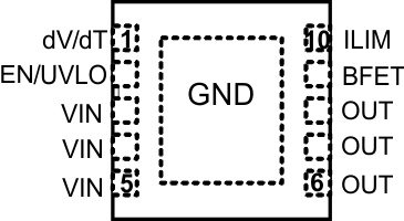
7 Pin Configuration and Functions
10-Pin VSON
DRC Package
(Top View)

Pin Functions
| PIN | DESCRIPTION | |
|---|---|---|
| NAME | NUMBER | |
| BFET | 9 | Connect this pin to the gate of a blocking NFET. See the Feature Description. |
| dV/dT | 1 | Tie a capacitor from this pin to GND to control the ramp rate of OUT at device turn-on. |
| EN/UVLO | 2 | This is a dual function control pin. When used as an ENABLE pin and pulled down, it shuts off the internal pass MOSFET and pulls BFET to GND. When pulled high, it enables the device and BFET. As an UVLO pin, it can be used to program different UVLO trip point via external resistor divider. |
| GND | PowerPAD™ | GND |
| ILIM | 10 | A resistor from this pin to GND will set the overload and short circuit limit. |
| OUT | 6-8 | Output of the device |
| VIN | 3-5 | Input supply voltage |