SLVSCE9D June 2014 – October 2017 TPS25942A , TPS25942L , TPS25944A , TPS25944L
UNLESS OTHERWISE NOTED, this document contains PRODUCTION DATA.
- 1 Features
- 2 Applications
- 3 Description
- 4 Revision History
- 5 Device Comparison Table
- 6 Pin Configuration and Functions
- 7 Specifications
- 8 Parameter Measurement Information
-
9 Detailed Description
- 9.1 Overview
- 9.2 Functional Block Diagram
- 9.3
Feature Description
- 9.3.1 Enable and Adjusting Undervoltage Lockout
- 9.3.2 Overvoltage Protection (OVP)
- 9.3.3 Hot Plug-In and In-Rush Current Control
- 9.3.4 Overload and Short Circuit Protection
- 9.3.5 Reverse Current Protection
- 9.3.6 FAULT Response
- 9.3.7 Current Monitoring
- 9.3.8 Power Good Comparator
- 9.3.9 IN, OUT and GND Pins
- 9.3.10 Thermal Shutdown
- 9.4 Device Functional Modes
-
10Application and Implementation
- 10.1 Application Information
- 10.2
Typical Application
- 10.2.1 Design Requirements
- 10.2.2
Detailed Design Procedure
- 10.2.2.1 Step by Step Design Procedure
- 10.2.2.2 Programming the Current-Limit Threshold: R(ILIM) Selection
- 10.2.2.3 Undervoltage Lockout and Overvoltage Set Point
- 10.2.2.4 Programming Current Monitoring Resistor—RIMON
- 10.2.2.5 Setting Output Voltage Ramp Time (tdVdT)
- 10.2.2.6 Programing the Power Good Set Point
- 10.2.2.7 Support Component Selections—R6, R7 and CIN
- 10.2.3 Application Curves
- 10.3 System Examples
- 11Power Supply Recommendations
- 12Layout
- 13Device and Documentation Support
- 14Mechanical, Packaging, and Orderable Information
Package Options
Mechanical Data (Package|Pins)
- RVC|20
Thermal pad, mechanical data (Package|Pins)
- RVC|20
Orderable Information
10.3.1.3 Priority MUXing With Almost Equal Rails (VIN1 ~ VIN2)
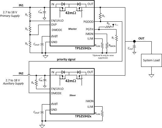
Most of the redundant power supply systems used in servers, storage and telecom, multiplex tightly regulated power rails to provide uninterrupted power to the load. In these systems, the primary and auxiliary rails are close to each other, typically within one diode drop when both rails are active.
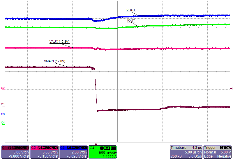
For priority multiplexing in these systems, the TPS25942 or TPS25944 device in auxiliary rail path can be operated in Diode Mode for a fast switch-over (1 µs typical). The fast switch-over reduces the required hold-up capacitor on the output rail for a given droop specification.
The circuit implementation of this configuration is shown in Figure 84. During power-fail (brown-out) conditions of primary rail IN1, it changes IN2 from ‘Diode-Mode’ to normal operation using PGOOD. Similarly during power recovery of primary rail IN1, the auxiliary rail IN2 is driven into ‘Diode-Mode’.
 Figure 84. Priority Power Multiplexing Configuration for Almost Equal Rails
The fast switch-over performance is shown in Figure 85.

| C(OUT) = 150 µF | RL = 4 Ω |