SLVSET8A May 2019 – August 2019 TPS2596
PRODUCTION DATA.
- 1 Features
- 2 Applications
- 3 Description
- 4 Revision History
- 5 Device Comparison Table
- 6 Pin Configuration and Functions
- 7 Specifications
-
8 Detailed Description
- 8.1 Overview
- 8.2 Functional Block Diagram
- 8.3 Feature Description
- 8.4 Device Functional Modes
-
9 Application and Implementation
- 9.1 Application Information
- 9.2
Typical Application
- 9.2.1 Precision Current Limiting and Protection for White Goods
- 9.2.2 Design Requirements
- 9.2.3 Detailed Design Procedure
- 9.2.4 Support Component Selection: RFLT and CIN
- 9.2.5 Application Curves
- 9.3 System Examples
- 10Power Supply Recommendations
- 11Layout
- 12Device and Documentation Support
- 13Mechanical, Packaging, and Orderable Information
Package Options
Mechanical Data (Package|Pins)
- DDA|8
Thermal pad, mechanical data (Package|Pins)
- DDA|8
Orderable Information
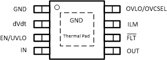
6 Pin Configuration and Functions
DDA Package
8-Pin SOIC
Top View

Pin Functions
| PIN | I/O | DESCRIPTION | |
|---|---|---|---|
| NAME | NO. | ||
| GND | 1 | Ground | Ground |
| dVdt | 2 | Analog Output | A capacitor from this pin to GND sets the output turn on slew rate. Leave this pin floating for the fastest turn on slew rate. |
| EN/UVLO | 3 | Analog Input | Active High Enable for the Device. A resistor divider can be used to adjust the Undervoltage Lockout threshold. Do not leave floating. |
| IN | 4 | Power | Power Input |
| OUT | 5 | Power | Power Output |
| FLT | 6 | Digital Output | Active Low indicator which will be pulled low when a fault is detected. It is an open-drain output that requires an external pull-up resistance. |
| ILM | 7 | Analog Output | This is a dual function pin used to limit and monitor the output current. An external resistor from this pin to GND sets the output current limit. The pin voltage can also be used to monitor the output load current. |
| OVLO | 8 | Analog Input | TPS25963x: A resistor divider can be used to adjust the Overvoltage Lockout threshold. Do not leave floating. |
| OVCSEL | TPS25962x: Overvoltage Clamp level select pin. Refer to Overvoltage Clamp for more details. | ||
| Thermal pad | Ground | The Exposed Pad is used primarily for heat dissipation and must be connected to system ground plane for best thermal performance. | |