SLVSGT8 December 2022 TPS25961
PRODUCTION DATA
- 1 Features
- 2 Applications
- 3 Description
- 4 Revision History
- 5 Pin Configuration and Functions
- 6 Specifications
-
7 Detailed Description
- 7.1 Overview
- 7.2 Functional Block Diagram
- 7.3 Feature Description
- 7.4 Device Functional Modes
- 8 Application and Implementation
- 9 Device and Documentation Support
- 10Mechanical, Packaging, and Orderable Information
Package Options
Mechanical Data (Package|Pins)
- DRV|6
Thermal pad, mechanical data (Package|Pins)
- DRV|6
Orderable Information
7.3.3.2 Active Current Limiting
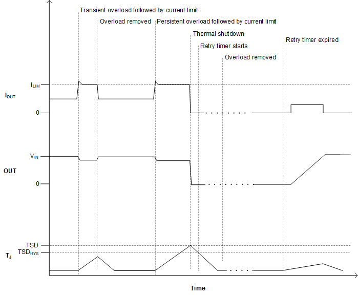
The device responds to output overcurrent conditions by actively limiting the current.
 Figure 7-5 TPS25961 Overcurrent
Response
Figure 7-5 TPS25961 Overcurrent
ResponseIn the current limiting state, the output voltage drops resulting in increased power dissipation in the internal FET leading to thermal shutdown if the condition persists for an extended period of time. In this case, the device performs 3 auto-retry attempts to allow the system to recover and then latches-off if the fault persists. See Fault response section for more details on device response after a fault.
The current limit threshold can be adjusted by pinstrapping the ILIM pin.
Use equation below to calculate the RILIM value for overcurrent thresholds < 200 mA.
Use equation below to calculate the RILIM value for overcurrent thresholds ≥ 200 mA.
- Leaving the ILIM pin open sets the current limit to its minimum value.
- The device scales the FET ON resistance in discrete steps according to the RILIM setting to provide optimum performance for the desired current level. At higher ILIM settings, the ON resistance is lower and at lower ILIM settings, the ON resistance is higher. However, for certain RILIM resistor values, the device may select an incorrect ON resistance scaling which is too high for the target load current leading to excessive voltage drop and power dissipation. To avoid this situation, it's recommended to avoid certain RILIM values as per Table 7-1.
| ILIM Resistor Value | Device ON Resistance |
|---|---|
| 250 kΩ < RILIM < 500 kΩ | Undefined |
| 111 kΩ < RILIM < 142 kΩ | Undefined |
| 58.8 kΩ < RILIM < 66.7 kΩ | Undefined |