SLVSFR1 August 2020 TPS25980
PRODUCTION DATA
- 1 Features
- 2 Applications
- 3 Description
- 4 Revision History
- 5 Device Comparison Table
- 6 Pin Configuration and Functions
- 7 Specifications
-
8 Detailed Description
- 8.1 Overview
- 8.2 Functional Block Diagram
- 8.3 Feature Description
- 8.4 Fault Response
- 8.5 Device Functional Modes
-
9 Application and Implementation
- 9.1 Application Information
- 9.2
Typical Application: Patient Monitoring System in Medical Applications
- 9.2.1 Design Requirements
- 9.2.2
Detailed Design Procedure
- 9.2.2.1 Device Selection
- 9.2.2.2 Setting the Current Limit Threshold: RILIM Selection
- 9.2.2.3 Setting the Undervoltage Lockout Set Point
- 9.2.2.4 Choosing the Current Monitoring Resistor: RIMON
- 9.2.2.5 Setting the Output Voltage Ramp Time (TdVdt)
- 9.2.2.6 Setting the Load Handshake (LDSTRT) Delay
- 9.2.2.7 Setting the Transient Overcurrent Blanking Interval (tITIMER)
- 9.2.2.8 Setting the Auto-Retry Delay and Number of Retries
- 9.2.3 Application Curves
- 9.3 System Examples
- 10Power Supply Recommendations
- 11Layout
- 12Device and Documentation Support
- 13Mechanical, Packaging, and Orderable Information
Package Options
Mechanical Data (Package|Pins)
- RGE|24
Thermal pad, mechanical data (Package|Pins)
- RGE|24
Orderable Information
9.3.1 Optical Module Power Rail Path Protection
Optical modules are commonly used in high-bandwidth data communication systems such as Optical Networking equipment, Enterprise/Data-Center Switches and Routers. Several variants of optical modules are available in the market, which differ in the form-factor and the data speed support (Gbit/s). Of these, the popular variant Double Dense Quad Small Form-factor Pluggable (QSFP-DD) module supports speeds up to 400 Gbit/s. In addition to the system protection during hot-plug events, the other key requirement for optical module is the tight voltage regulation. The optical module uses 3.3 V supply and requires voltage regulation within ±5 % for proper operation.
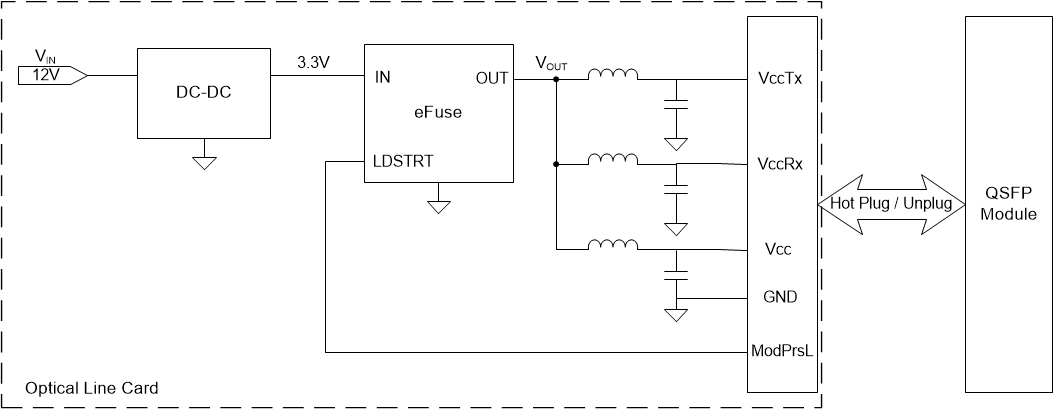
A typical power tree of such system is shown in Figure 9-13. The optical line card consists of DC-DC converter, protection device (eFuse) and power supply filters. The DC-DC converter steps-down the 12 V to 3.3 V and maintains the 3.3 V rail within ±2 %. The power supply filtering network uses ‘LC’ components to reduce high frequency noise injection into the optical module. The DC resistance of the inductor ‘L’ causes voltage drop of around 1.5 % which leaves us with a voltage drop budget of just 1.5 % (3.3 V * 1.5% = 50 mV) across the protection device. Considering a maximum load current of 5.5 A per module, the maximum ON-resistance of the protection device should be less than 9 mΩ. TPS25980x eFuse offers ultra-low ON-resistance of 2.7 mΩ (typical) and 4.5 mΩ (maximum, across temperature), thereby meeting the target specification with additional margin to spare and simplifying the overall system design.
 Figure 9-13 Power Tree Block Diagram of a Typical Optical Line Card
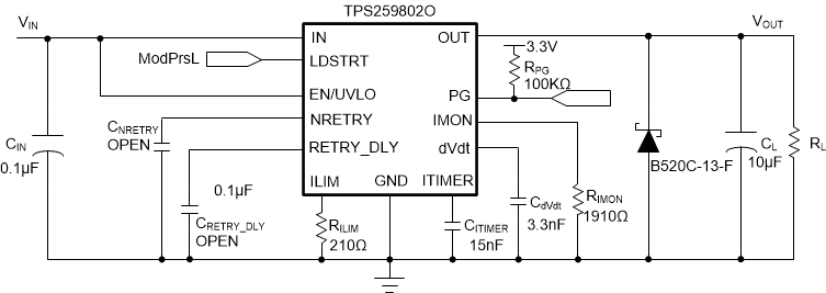
As shown in Figure 9-13, ModPrsL signal acts as a handshake signal between the line card and the optical module. ModPrsL is always pulled to ground inside the module. When the module is hot-plugged into the host “Optical Line Card” connector, the ModPrsL signal pulls down the LDSTRT pin and enables the TPS25980x eFuse to power the module. This ensures that power is applied on the port only when a module is plugged in and disconnected when there is no module present.
 Figure 9-14 TPS259802O Configured for a 3.3-V Power Rail Path Protection in Optical Module