SLVSGG6B april 2022 – june 2023 TPS25981
PRODUCTION DATA
- 1
- 1 Features
- 2 Applications
- 3 Description
- 4 Revision History
- 5 Device Comparison Table
- 6 Pin Configuration and Functions
- 7 Specifications
-
8 Detailed Description
- 8.1 Overview
- 8.2 Functional Block Diagram
- 8.3
Feature Description
- 8.3.1 Undervoltage Lockout (UVLO and UVP)
- 8.3.2 Overvoltage Lockout (OVLO)
- 8.3.3 Inrush Current, Overcurrent, and Short-Circuit Protection
- 8.3.4 Analog Load Current Monitor
- 8.3.5 Overtemperature Protection (OTP)
- 8.3.6 Fault Response and Indication (FLT)
- 8.3.7 Power Good Indication (PG)
- 8.3.8 Quick Output Discharge (QOD)
- 8.3.9 Reverse Current Blocking FET Driver
- 8.4 Device Functional Modes
- 9 Application and Implementation
- 10Power Supply Recommendations
- 11Layout
- 12Device and Documentation Support
- 13Mechanical, Packaging, and Orderable Information
Package Options
Mechanical Data (Package|Pins)
- RPW|10
Thermal pad, mechanical data (Package|Pins)
Orderable Information
8.3.3.4 Short-Circuit Protection
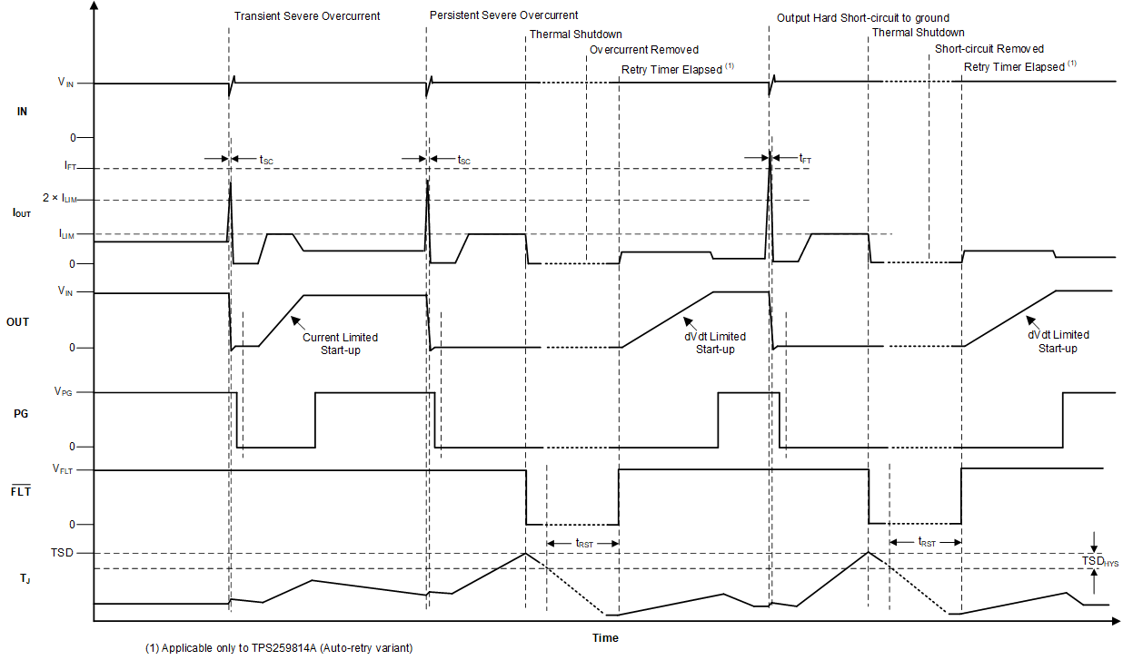
During an output short-circuit event, the current through the device increases very rapidly. When a severe overcurrent condition is detected, the device triggers a fast-trip response to limit the current to a safe level. The internal fast-trip comparator employs a scalable threshold (ISC) which is equal to 2 × ILIM. This action enables the user to adjust the fast-trip threshold rather than using a fixed threshold which can be too high for some low current systems. The device also employs a fixed fast-trip threshold (IFT) to protect fast protection against hard short circuits during steady-state. The fixed fast-trip threshold is higher than the maximum recommended user adjustable scalable fast-trip threshold. After the current exceeds ISC or IFT, the FET is turned off completely within tFT. Thereafter, the devices tries to turn the FET back on after a short de-glitch interval (30 μs) in a current limited manner instead of a dVdt limited manner. This action ensures that the FET has a faster recovery after a transient overcurrent event and minimizes the output voltage droop. However, if the fault is persistent, the device stays in current limit causing the junction temperature to rise and eventually enter thermal shutdown. For details on the device response to overtemperature, see Overtemperature Protection (OTP).
 Figure 8-5 TPS25981xx Short-Circuit Response