SLVSGX1A July 2023 – October 2023 TPS25984
PRODUCTION DATA
- 1
- 1 Features
- 2 Applications
- 3 Description
- 4 Revision History
- 5 Description (continued)
- 6 Pin Configuration and Functions
- 7 Specifications
-
8 Detailed Description
- 8.1 Overview
- 8.2 Functional Block Diagram
- 8.3
Feature Description
- 8.3.1 Undervoltage Protection
- 8.3.2 Insertion Delay
- 8.3.3 Overvoltage Protection
- 8.3.4 Inrush Current, Overcurrent, and Short-Circuit Protection
- 8.3.5 Analog Load Current Monitor (IMON)
- 8.3.6 Mode Selection (MODE)
- 8.3.7 Parallel Device Synchronization (SWEN)
- 8.3.8 Stacking Multiple eFuses for Unlimited Scalability
- 8.3.9 Analog Junction Temperature Monitor (TEMP)
- 8.3.10 Overtemperature Protection
- 8.3.11 Fault Response and Indication (FLT)
- 8.3.12 Power-Good Indication (PG)
- 8.3.13 Output Discharge
- 8.3.14 FET Health Monitoring
- 8.3.15 Single Point Failure Mitigation
- 8.4 Device Functional Modes
- 9 Application and Implementation
- 10Device and Documentation Support
- 11Mechanical, Packaging, and Orderable Information
Package Options
Mechanical Data (Package|Pins)
- RZJ|32
Thermal pad, mechanical data (Package|Pins)
- RZJ|32
Orderable Information
3 Description
The TPS25984x is an integrated, high-current circuit protection and power management solution in a small package. The device provides multiple protection modes using very few external components and is a robust defense against overloads, short circuits, and excessive inrush current.
Applications with particular inrush current requirements can set the output slew rate with a single external capacitor. Output current limit level can be set by user as per system needs. A user adjustable overcurrent blanking timer allows systems to support transient peaks in the load current without tripping the eFuse.
Device Information
| PART NUMBER | PACKAGE(1) | PACKAGE SIZE (NOM)(2) |
|---|---|---|
| TPS259840RZJ | RZJ (QFN, 32) | 5 mm × 5 mm |
| TPS259841RZJ |
(1) For all available packages, see the orderable addendum at the end of the data sheet.
(2) The package size (length × width) is a nominal value and includes pins, where
applicable
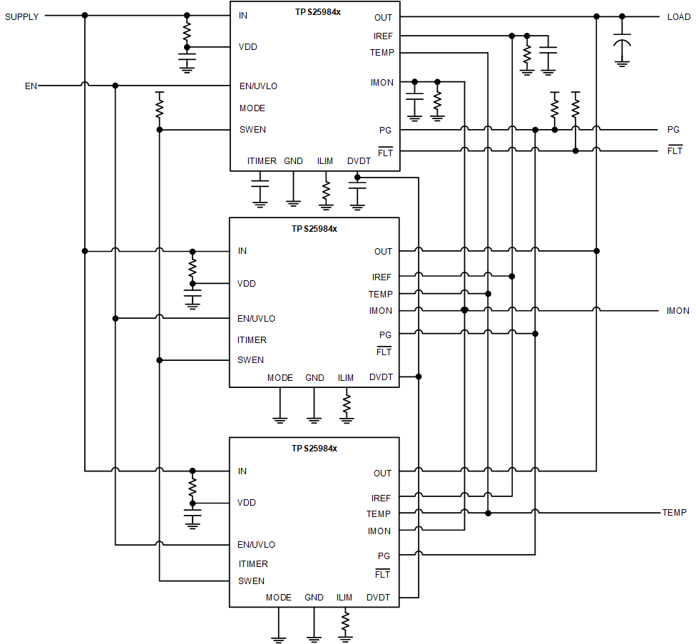
 Simplified schematic