SLVSGG3A May   2022  – September 2022 TPS25985

PRODUCTION DATA  

  1. Features
  2. Applications
  3. Description
  4. Revision History
  5. Description (continued)
  6. Pin Configuration and Functions
  7. Specifications
    1. 7.1 Absolute Maximum Ratings
    2. 7.2 ESD Ratings
    3. 7.3 Recommended Operating Conditions
    4. 7.4 Thermal Information
    5. 7.5 Electrical Characteristics
    6. 7.6 Logic Interface
    7. 7.7 Timing Requirements
    8. 7.8 Switching Characteristics
    9. 7.9 Typical Characteristics
  8. Detailed Description
    1. 8.1 Overview
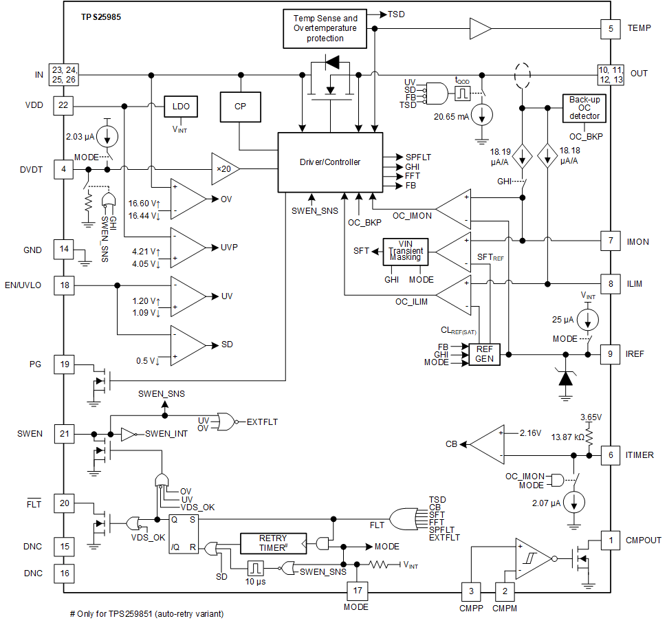
    2. 8.2 Functional Block Diagram
    3. 8.3 Feature Description
      1. 8.3.1  Undervoltage Protection
      2. 8.3.2  Insertion Delay
      3. 8.3.3  Overvoltage Protection
      4. 8.3.4  Inrush Current, Overcurrent, and Short-Circuit Protection
        1. 8.3.4.1 Slew rate (dVdt) and Inrush Current Control
          1. 8.3.4.1.1 Start-Up Time Out
        2. 8.3.4.2 Steady-State Overcurrent Protection (Circuit-Breaker)
        3. 8.3.4.3 Active Current Limiting During Start-Up
        4. 8.3.4.4 Short-Circuit Protection
      5. 8.3.5  Analog Load Current Monitor (IMON)
      6. 8.3.6  Mode Selection (MODE)
      7. 8.3.7  Parallel Device Synchronization (SWEN)
      8. 8.3.8  Stacking Multiple eFuses for Unlimited Scalability
        1. 8.3.8.1 Current Balancing During Start-Up
      9. 8.3.9  Analog Junction Temperature Monitor (TEMP)
      10. 8.3.10 Overtemperature Protection
      11. 8.3.11 Fault Response and Indication (FLT)
      12. 8.3.12 Power Good Indication (PG)
      13. 8.3.13 Output Discharge
      14. 8.3.14 General Purpose Comparator
      15. 8.3.15 FET Health Monitoring
      16. 8.3.16 Single Point Failure Mitigation
        1. 8.3.16.1 IMON Pin Single Point Failure
        2. 8.3.16.2 ILIM Pin Single Point Failure
        3. 8.3.16.3 IREF Pin Single Point Failure
        4. 8.3.16.4 ITIMER Pin Single Point Failure
    4. 8.4 Device Functional Modes
  9. Application and Implementation
    1. 9.1 Application Information
      1. 9.1.1 Single Device, Standalone Operation
      2. 9.1.2 Multiple Devices, Parallel Connection
    2. 9.2 Typical Application: 12-V, 3.6-kW Power Path Protection in Datacenter Servers
      1. 9.2.1 Application
      2. 9.2.2 Design Requirements
      3. 9.2.3 Detailed Design Procedure
      4. 9.2.4 Application Performance Plots
    3. 9.3 Multiple eFuses, Parallel Connection with PMBus
    4. 9.4 Digital Telemetry Using External Microcontroller
    5. 9.5 What to Do and What Not to Do
  10. 10Power Supply Recommendations
    1. 10.1 Transient Protection
    2. 10.2 Output Short-Circuit Measurements
  11. 11Layout
    1. 11.1 Layout Guidelines
    2. 11.2 Layout Example
  12. 12Device and Documentation Support
    1. 12.1 Documentation Support
      1. 12.1.1 Related Documentation
    2. 12.2 Receiving Notification of Documentation Updates
    3. 12.3 Support Resources
    4. 12.4 Trademarks
    5. 12.5 Electrostatic Discharge Caution
    6. 12.6 Glossary
  13. 13Mechanical, Packaging, and Orderable Information

Package Options

Mechanical Data (Package|Pins)
Thermal pad, mechanical data (Package|Pins)
Orderable Information

Functional Block Diagram

GUID-20211230-SS0I-HH79-3FX9-7LLNW0JQXJKR-low.gif