SLVSFQ6A November 2020 – June 2021 TPS2640
PRODUCTION DATA
- 1 Features
- 2 Applications
- 3 Description
- 4 Revision History
- 5 Device Comparison
- 6 Pin Configuration and Functions
- 7 Specifications
- 8 Parameter Measurement Information
-
9 Detailed Description
- 9.1 Overview
- 9.2 Functional Block Diagram
- 9.3
Feature Description
- 9.3.1 Undervoltage Lockout (UVLO)
- 9.3.2 Overvoltage Protection (OVP)
- 9.3.3 Reverse Input Supply Protection
- 9.3.4 Hot Plug-In and In-Rush Current Control
- 9.3.5 Overload and Short Circuit Protection
- 9.4 Device Functional Modes
-
10Application and Implementation
- 10.1 Application Information
- 10.2 Typical Application
- 10.3 System Examples
- 10.4 Do's and Dont's
- 11Power Supply Recommendations
- 12Layout
- 13Device and Documentation Support
- 14Mechanical, Packaging, and Orderable Information
Package Options
Mechanical Data (Package|Pins)
Thermal pad, mechanical data (Package|Pins)
- PWP|16
Orderable Information
9.3.2 Overvoltage Protection (OVP)
The TPS26400 incorporate circuitry to protect the system during overvoltage conditions. A voltage more than V(OVPR) on OVP pin turns off the internal FET and protects the downstream load. To program the OVP threshold externally, connect a resistor divider from IN supply to OVP terminal to RTN as shown in Figure 9-1. The TPS26400 also feature a factory set 33-V Input overvoltage cut off V(IN_OVP) threshold with a 2-V hysteresis. This feature can be enabled by connecting the OVP terminal directly to the RTN terminal. Figure 7-26 illustrates the overvoltage cut-off functionality.
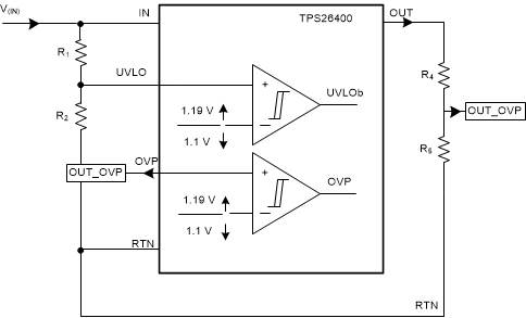
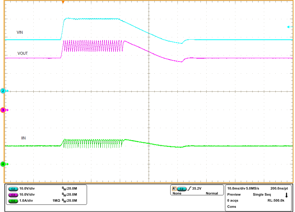
Programmable output overvoltage clamp can also be achieved using TPS26400 by connecting the resistor ladder
from Vout to OVP to RTN as shown in Figure 9-2 . This results in clamping of output voltage close to OVP setpoint
by resistors R4 and R5. as shown in Figure 9-3. This scheme will also help in achieving minimal system Iq
during off state. For this OVP configurataion, use R4 > 90 kΩ.
 Figure 9-2 Programmable Output OV Clamp
 Figure 9-3 Programmable Output Overvoltage Clamp Response