SLVSH35A October 2023 – February 2024 TPS274C65CP
PRODUCTION DATA
- 1
- 1 Features
- 2 Applications
- 3 Description
- 4 Device Comparison Table
- 5 Pin Configuration and Functions
- 6 Specifications
- 7 Parameter Measurement Information
-
8 Detailed Description
- 8.1 Overview
- 8.2 Functional Block Diagram
- 8.3
Feature Description
- 8.3.1 Pin Diagrams
- 8.3.2 Programmable Current Limit
- 8.3.3
Protection Mechanisms
- 8.3.3.1 Over-current Protection
- 8.3.3.2 Short-Circuit Protection
- 8.3.3.3 Thermal Shutdown Behavior
- 8.3.3.4 Inductive-Load Switching-Off Clamp
- 8.3.3.5 Inductive Load Demagnetization
- 8.3.3.6 Thermal Shutdown
- 8.3.3.7 Undervoltage Protection on VS (UVP)
- 8.3.3.8 Undervoltage Lockout on Low Voltage Supply (VDD_UVLO)
- 8.3.3.9 Power-Up and Power-Down Behavior
- 8.3.4 Diagnostic Mechanisms
- 8.4 Device Functional Modes
- 9 Application and Implementation
- 10Device and Documentation Support
- 11Revision History
- 12Mechanical, Packaging, and Orderable Information
Package Options
Mechanical Data (Package|Pins)
- RHA|40
Thermal pad, mechanical data (Package|Pins)
- RHA|40
Orderable Information
9.2.3 Application Curves
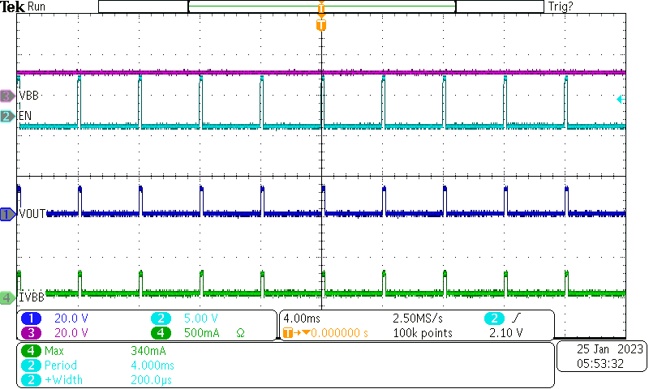
Figure 9-2 shows a test example of switching the load with 250 kHz PWM signal. Test conditions: VS =12 V, Duty Cycle = 5%, TAMB = 25 °C. Channel 1 is VOUT voltage. Channel 2 is EN pin voltage. Channel 3 is VS voltage. Channel 4 is VS current.
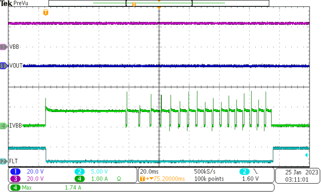
Figure 9-3 shows a test example of enabling a switch while there is a short at the output. Test conditions: VS = 24 V, TAMB = 25 °C. Channel 1 is VOUT voltage. Channel 2 is FAULT pin voltage. Channel 3 is VS voltage. Channel 4 is VS current.
 Figure 9-2 250 kHz PWM
Switching
 Figure 9-3 Enable into Short
Circuit