SLUSAR9D December 2011 – December 2021 TPS28225-Q1
PRODUCTION DATA
- 1 Features
- 2 Applications
- 3 Description
- 4 Revision History
- 5 Pin Configuration and Functions
- 6 Specifications
- 7 Detailed Description
- 8 Application and Implementation
- 9 Power Supply Recommendations
- 10Layout
- 11Device and Documentation Support
- 12Mechanical, Packaging, and Orderable Information
Package Options
Mechanical Data (Package|Pins)
Thermal pad, mechanical data (Package|Pins)
- DRB|8
Orderable Information
8.2.1 Design Requirements
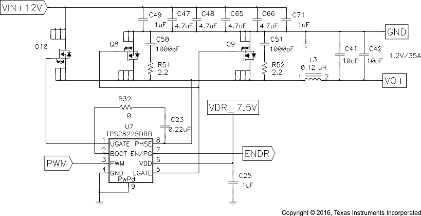
The DC-DC converter in Figure 8-4 displays the schematic of the TPS28225 in a multiphase high-current step-down power supply (only one phase is shown). This example schematic uses a single high-side MOSFET and two low-side MOSFETs the latter connected in parallel. The TPS28225 is controlled by multiphase buck DC/DC controller like TPS40090-Q1. As TPS28225 has internal shoot-through protection, only one PWM control signal is required for each channel.
The VRM example schematic is capable of driving 35 A per phase. In this example it has a nominal input voltage of 12 V within a tolerance range of ±5%. The switching frequency is 500 kHz. The nominal duty cycle is 10%, therefore the low-side MOSFETs are conducting 90% of the time. By choosing lower RDS(on) the conduction losses of the switching elements are minimized. The TPS28225 is controlled by multiphase buck DC/DC controller like TPS40090-Q1.
| DESIGN PARAMETER | VALUE |
|---|---|
| Supply Voltage | 12 V ± 5% |
| Output Voltage | 0.83 V to 1.6 V |
| Frequency | 500 kHz |
| Efficiency | 87% |
| Peak-to-peak voltage on load current (0 A –90 A ) | <160 mV |
