SLUSAR9D December 2011 – December 2021 TPS28225-Q1
PRODUCTION DATA
- 1 Features
- 2 Applications
- 3 Description
- 4 Revision History
- 5 Pin Configuration and Functions
- 6 Specifications
- 7 Detailed Description
- 8 Application and Implementation
- 9 Power Supply Recommendations
- 10Layout
- 11Device and Documentation Support
- 12Mechanical, Packaging, and Orderable Information
Package Options
Mechanical Data (Package|Pins)
Thermal pad, mechanical data (Package|Pins)
- DRB|8
Orderable Information
3 Description
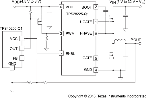
The TPS28225-Q1 is a high-speed driver for N-channel complementary driven power MOSFETs with adaptive dead-time control. This driver is optimized for use in variety of high-current, single and multi-phase DC-to-DC converters. The TPS28225-Q1 is highly efficient, has a small solution size and low-EMI emissions.
The TPS28225-Q1 device offers high performance features such as a 8.8-V gate drive voltage, 14-ns adaptive dead-time control, 14-ns propagation delays and high-current 2-A source and 4-A sink drive capabilities. The 0.4-Ω impedance for the lower gate driver holds the gate of power MOSFET below its threshold and ensures no shoot-through current at high dV/dt phase node transitions. The bootstrap capacitor is charged by an internal diode which allows the use of an N-channel MOSFETs in a half-bridge configuration.
The TPS28225-Q1 is offered in an economical SOIC-8 package and in a thermally enhanced small sized VSON package. The driver is specified to operate in the temperature range of –40°C to 105°C with the absolute maximum junction temperature of 150°C.
| PART NUMBER | PACKAGE | BODY SIZE (NOM) |
|---|---|---|
| TPS28225-Q1 | SOIC (8) | 5.00 mm × 6.20 mm |
| VSON (8) | 3.00 mm × 3.00 mm |
 Simplified Schematic