SLUS710E May 2006 – January 2024 TPS28225
PRODUCTION DATA
- 1
- 1 Features
- 2 Applications
- 3 Description
- 4 Pin Configuration and Functions
- 5 Specifications
- 6 Detailed Description
- 7 Application and Implementation
- 8 Power Supply Recommendations
- 9 Layout
- 10Device and Documentation Support
- 11Revision History
- 12Mechanical, Packaging, and Orderable Information
Package Options
Mechanical Data (Package|Pins)
Thermal pad, mechanical data (Package|Pins)
- DRB|8
Orderable Information
6.3.3 Enable/Power Good
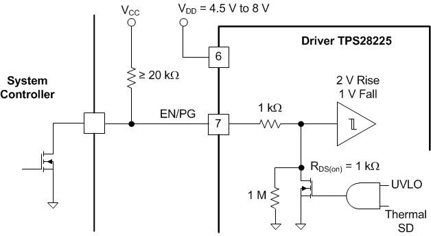
The Enable/Power Good circuit allows the TPS28225 to follow the PWM input signal when the voltage at EN/PG pin is above 2.1 V maximum. This circuit has a unique two-way communication capability. This is illustrated by Figure 6-1.
 Figure 6-1 Enable/Power Good Circuit
The EN/PG pin has approximately 1-kΩ internal series resistor. Pulling EN/PG high by an external ≥ 20-kΩ resistor allows two-way communication between controller and driver. If the input voltage VDD is below UVLO threshold or thermal shut down occurs, the internal MOSFET pulls EN/PG pin to GND through 1-kΩ resistor. The voltage across the EN/PG pin is now defined by the resistor divider comprised by the external pull up resistor, 1-kΩ internal resistor and the internal FET having 1-kΩ RDS(on). Even if the system controller allows the driver to start by setting its own enable output transistor OFF, the driver keeps the voltage at EN/PG low. Low EN/PG signal indicates that the driver is not ready yet because the supply voltage VDD is low or that the driver is in thermal shutdown mode. The system controller can arrange the delay of PWM input signals coming to the driver until the driver releases EN/PG pin. If the input voltage VDD is back to normal, or the driver is cooled down below its lower thermal shutdown threshold, then the internal MOSFET releases the EN/PG pin and normal operation resumes under the external Enable signal applied to EN/PG input. Another feature includes an internal 1-MΩ resistor that pulls EN/PG pin low and disables the driver in case the system controller accidentally loses connection with the driver. This could happen if, for example, the system controller is located on a separate PCB daughter board.
The EN/PG pin can serve as the second pulse input of the driver additionally to PWM input. The delay between EN/PG and the UGATE going high, provided that PWM input is also high, is only about 30 ns. If the PWM input pulses are synchronized with EN/PG input, then when PWM and EN/PG are high, the UGATE is high and LGATE is low. If both PWM and EN/PG are low, then UGATE and LGATE are both low as well. This means the driver allows operation of a synchronous buck regulator as a conventional buck regulator using the body diode of the low-side power MOSFET as the freewheeling diode. This feature can be useful in some specific applications to allow startup with a pre-biased output or, to improve the efficiency of buck regulator when in power saving mode with low output current.