SLUS710E May 2006 – January 2024 TPS28225
PRODUCTION DATA
- 1
- 1 Features
- 2 Applications
- 3 Description
- 4 Pin Configuration and Functions
- 5 Specifications
- 6 Detailed Description
- 7 Application and Implementation
- 8 Power Supply Recommendations
- 9 Layout
- 10Device and Documentation Support
- 11Revision History
- 12Mechanical, Packaging, and Orderable Information
Package Options
Mechanical Data (Package|Pins)
Thermal pad, mechanical data (Package|Pins)
- DRB|8
Orderable Information
7.2.2.1 Four Phases Driven by TPS28225 Driver
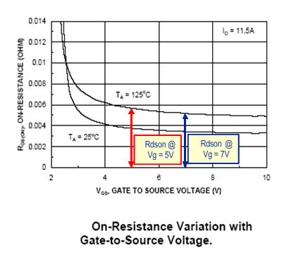
When using the same power stage Figure 7-1, the driver with the optimal drive voltage and optimal dead time can boost efficiency up to 5%. The optimal 8-V drive voltage versus 5-V drive contributes 2% to 3% efficiency increase and the remaining 1% to 2% can be attributed to the reduced dead time. The 7-V to 8-V drive voltage is optimal for operation at switching frequency range above 400 kHz and can be illustrated by observing typical RDS(on) curves of modern FETs as a function of their gate-drive voltage. This is shown in Figure 7-2.
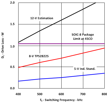
Figure 7-2 and Figure 7-3 show that the RDS(on) at 5-V drive is substantially larger than at 7 V and above that the RDS(on) curve is almost flat. This means that moving from 5-V drive to an 8-V drive boosts the efficiency because of lower RDS(on) of the MOSFETs at 8 V. Further increase of drive voltage from 8 V to 12 V only slightly decreases the conduction losses but the power dissipated inside the driver increases dramatically (by 125%). The power dissipated by the driver with 5-V, 8-V and 12-V drive as a function of switching frequency from 400 kHz to 800 kHz. It should be noted that the 12-V driver exceeds the maximum dissipated power allowed for an SOIC-8 package even at 400-kHz switching frequency.

