SLUS791A July 2007 – September 2015 TPS28226
PRODUCTION DATA.
- 1 Features
- 2 Applications
- 3 Description
- 4 Revision History
- 5 Pin Configuration and Functions
- 6 Specifications
- 7 Detailed Description
- 8 Application and Implementation
- 9 Power Supply Recommendations
- 10Layout
- 11Device and Documentation Support
- 12Mechanical, Packaging, and Orderable Information
Package Options
Mechanical Data (Package|Pins)
Thermal pad, mechanical data (Package|Pins)
- DRB|8
Orderable Information
8 Application and Implementation
NOTE
Information in the following applications sections is not part of the TI component specification, and TI does not warrant its accuracy or completeness. TI’s customers are responsible for determining suitability of components for their purposes. Customers should validate and test their design implementation to confirm system functionality.
8.1 Application Information
To effect fast switching of power devices and reduce associated switching power losses, a powerful MOSFET driver is employed between the PWM output of controllers and the gates of the power semiconductor devices. Also, MOSFET drivers are indispensable when it is impossible for the PWM controller to directly drive the MOSFETs of the switching devices. With the advent of digital power, this situation will be often encountered because the PWM signal from the digital controller is often a 3.3-V logic signal which cannot effectively turn on a power switch. Level shifting circuitry is needed to boost the 3.3-V signal to the gate-drive voltage (such as 12 V) in order to fully turn on the power device and minimize conduction losses. Traditional buffer drive circuits based on NPN/PNP bipolar transistors in totem-pole arrangement, being emitter follower configurations, prove inadequate with digital power because they lack level-shifting capability. MOSFET drivers effectively combine both the level-shifting and buffer-drive functions.
MOSFET drivers also find other needs such as minimizing the effect of high-frequency switching noise by locating the high-current driver physically close to the power switch, driving gate-drive transformers and controlling floating power-device gates, reducing power dissipation and thermal stress in controllers by moving gate charge power losses from the controller into the driver.
8.2 Typical Application
The DC-DC converter in Figure 25 displays the schematic of the TPS28226 in a multiphase high-current step-down power supply (only one phase is shown). This design uses a single high-side MOSFET Q10 and two low-side MOSFETs Q8 and Q9, the latter connected in parallel. The TPS28226 is controlled by multiphase buck DC-to-DC controller like TPS40090. As TPS28226 has internal shoot-through protection only one PWM control signal is required for each channel.
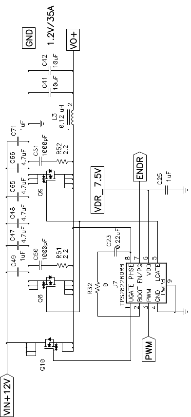 Figure 25. One of Four Phases Driven by TPS28226 Driver in 4-Phase VRM Reference Design
8.2.1 Design Requirements
The VRM Reference Design is capable of driving 35 A per phase. In this example it has a nominal input voltage of 12 V within a tolerance range of ±5%. The switching frequency is 500 kHz. The nominal duty cycle is 10%, therefore the low-side MOSFETs are conducting 90% of the time. By choosing lower RDS(on) the conduction losses of the switching elements are minimized.
Table 2. VRM Reference Design Requirements
| DESIGN PARAMETER | VALUE |
|---|---|
| Supply voltage | 12 V ±5% |
| Output voltage | 0.83 V to 1.6 V |
| Frequency | 500 kHz |
| Peak-to-peak output voltage variation on load current transient (0 A to 100 A ) within 1 µs | <160 mV |
| Dynamic output voltage change slew rate | 12.25 mV per 5 µs |
8.2.2 Detailed Design Procedure
The bootstrap current can be limited by changing R32 to prevent overcharging of the bootstrap capacitor and to slow the turn-on transition of the high-side MOSFET. This reduces the peak amplitude and ringing of the switching node. Furthermore it minimizes the possibility of Cdv/dt-induced shoot-through of the low-side MOSFETs. The snubbers composed of C50 with R51 and C51 with R52 help to reduce switching noise.
The output component selection considers the requirement of a fast transient response. For output capacitors small capacitance values are chosen because of rapid changes of the output voltage. These changes also require an inductor with low inductance. Due to the small duty cycle the low-side MOSFETs conduct a long time. Two low-side MOSFETs are selected to increase both thermal performance and efficiency.
8.2.2.1 Four Phases Driven by TPS28226 Driver
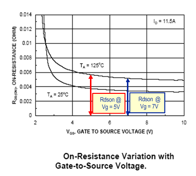
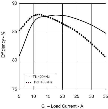
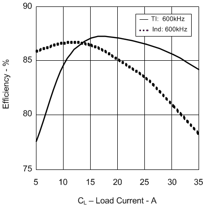
When using the same power stage Figure 25, the driver with the optimal drive voltage and optimal dead time can boost efficiency up to 5%. The optimal 8-V drive voltage versus 5-V drive contributes 2% to 3% efficiency increase and the remaining 1% to 2% can be attributed to the reduced dead time. The 7-V to 8-V drive voltage is optimal for operation at switching frequency range above 400 kHz and can be illustrated by observing typical RDS(on) curves of modern FETs as a function of their gate-drive voltage. This is shown in Figure 26.
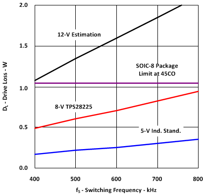
Figure 26 and Figure 27 show that the RDS(on) at 5-V drive is substantially larger than at 7 V and above that the RDS(on) curve is almost flat. This means that moving from 5-V drive to an 8-V drive boosts the efficiency because of lower RDS(on) of the MOSFETs at 8 V. Further increase of drive voltage from 8 V to 12 V only slightly decreases the conduction losses but the power dissipated inside the driver increases dramatically (by 125%). The power dissipated by the driver with 5-V, 8-V and 12-V drive as a function of switching frequency from 400 kHz to 800 kHz. It should be noted that the 12-V driver exceeds the maximum dissipated power allowed for an SOIC-8 package even at 400-kHz switching frequency.
8.2.2.2 Switching The MOSFETs
Driving the MOSFETs efficiently at high switching frequencies requires special attention to layout and the reduction of parasitic inductances. Efforts need to be done both at the driver’s die and package level and at the PCB layout level to keep the parasitic inductances as low as possible. Figure 28 shows the main parasitic inductances and current flow during turning ON and OFF of the MOSFET by charging its CGS gate capacitance.
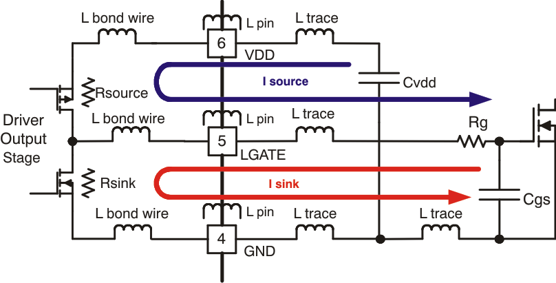 Figure 28. MOSFET Drive Paths and Main Circuit Parasitics
The ISOURCE current charges the gate capacitor and the ISINK current discharges it. The rise and fall time of voltage across the gate defines how quickly the MOSFET can be switched. The timing parameters specified in datasheet for both upper and lower driver are shown in Figure 16 and Figure 17 where 3-nF load capacitor has been used for the characterization data. Based on these actual measurements, the analytical curves in Figure 29 and Figure 30 show the output voltage and current of upper and low side drivers during the discharging of load capacitor. The left waveforms show the voltage and current as a function of time, while the right waveforms show the relation between the voltage and current during fast switching. These waveforms show the actual switching process and its limitations because of parasitic inductances. The static VOUT/ IOUT curves shown in many datasheets and specifications for the MOSFET drivers do not replicate actual switching condition and provide limited information for the user.
Turning Off of the MOSFET needs to be done as fast as possible to reduce switching losses. For this reason the TPS28226 driver has very low output impedance specified as 0.4 Ω typical for lower driver and 1 Ω typical for upper driver at DC current. Assuming 8-V drive voltage and no parasitic inductances, one can expect an initial sink current amplitude of 20 A and 8 A respectively for the lower and upper drivers. With pure R-C discharge circuit for the gate capacitor, the voltage and current waveforms are expected to be exponential. However, because of parasitic inductances, the actual waveforms have some ringing and the peak current for the lower driver is about 4 A and about 2.5 A for the upper driver (Figure 29 and Figure 30). The overall parasitic inductance for the lower drive path is estimated as 4 nH and for the upper drive path as 6 nH. The internal parasitic inductance of the driver, which includes inductances of bonded wires and package leads, can be estimated for SOIC-8 package as 2 nH for lower gate and 4 nH for the upper gate. Use of DFN-8 package reduces the internal parasitic inductances by approximately 50%.
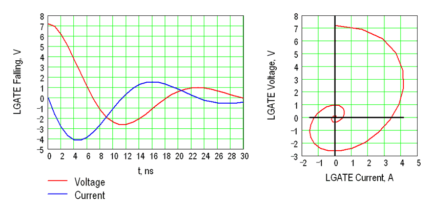 Figure 29. LGATE Turning Off Voltage and Sink Current vs Time (Related Switching Diagram (right))
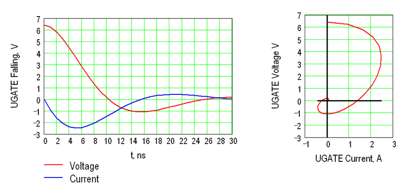 Figure 30. UGATE Turning Off Voltage and Sink Current vs Time (Related Switching Diagram (right))
8.2.2.3 List of Materials
For this specific example see Table 3. The component vendors are not limited to those shown in the table below. It should be noted that in this example, the power MOSFET packages were chosen with drains on top. The decoupling capacitors C47, C48, C65, and C66 were chosen to have low profiles. This allows the designer to meet good layout rules and place a heatsink on top of the FETs using an electrically isolated and thermally conductive pad.
Table 3. List of Materials
| REF DES | COUNT | DESCRIPTION | MANUFACTURE | PART NUMBER |
|---|---|---|---|---|
| C47, C48, C65, C66 | 4 | Capacitor, ceramic, 4.7 μF, 16 V, X5R 10%, low profile 0.95 mm, 1206 | TDK | C3216X5R1C475K |
| C41, C42 | 2 | Capacitor, ceramic, 10 μF, 16 V, X7R 10%, 1206 | TDK | C3216X7R1C106K |
| C50, C51 | 2 | Capacitor, ceramic, 1000 pF, 50 V, X7R, 10%, 0603 | Std | Std |
| C23 | 1 | Capacitor, ceramic, 0.22 μF, 16 V, X7R, 10%, 0603 | Std | Std |
| C25, C49, C71 | 3 | Capacitor, ceramic, 1 μF, 16 V, X7R, 10%, '0603 | Std | Std |
| L3 | 1 | Inductor, SMT, 0.12 μH, 31 A, 0.36 mΩ, 0.400 x 0.276 | Pulse | PA0511-101 |
| Q8, Q9 | 2 | Mosfet, N-channel, VDS 30 V, RDS 2.4 mΩ, ID 45 A, LFPAK-i | Renesas | RJK0301DPB-I |
| Q10 | 1 | Mosfet, N-channel, VDS 30 V, RDS 6.2 mΩ, ID 30 A, LFPAK-i | Renesas | RJK0305DPB-I |
| R32 | 1 | Resistor, chip, 0 Ω, 1/10 W, 1%, '0805 | Std | Std |
| R51, R52 | 2 | Resistor, chip, 2.2 Ω, 1/10 W, 1%, '0805 | Std | Std |
| U7 | 1 | Device, High Frequency 4-A Sink Synchronous Buck MOSFET Driver, DFN-8 | Texas Instruments | TPS28226DRB |
8.2.3 Application Curves
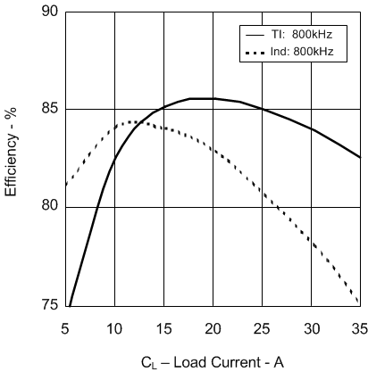
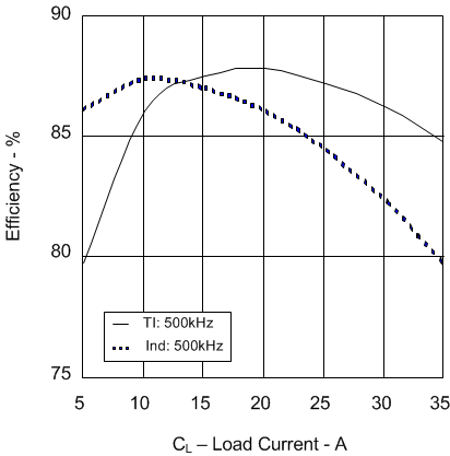
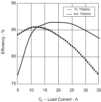
Efficiency achieved using TPS28226 driver with 8-V drive at different switching frequencies a similar industry 5-V driver using the power stage in Figure 25 is shown in Figure 31, Figure 32, Figure 33, Figure 34 and Figure 35.
8.3 System Examples
Figure 36, Figure 37 and Figure 38 below illustrate typical implementations of the TPS28226 in step-down power supplies.
 Figure 36. One-Phase POL Regulator
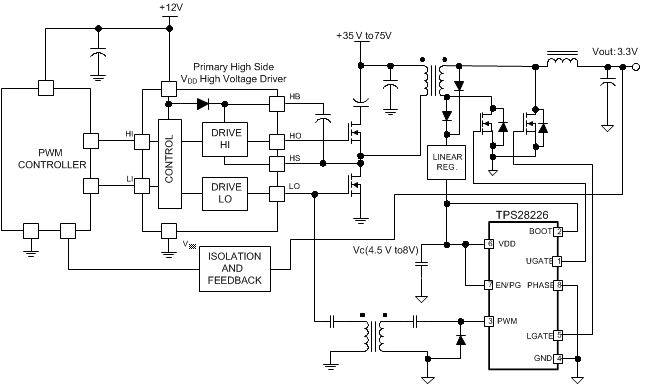 Figure 37. Driver for Synchronous Rectification with Complementary Driven MOSFETs
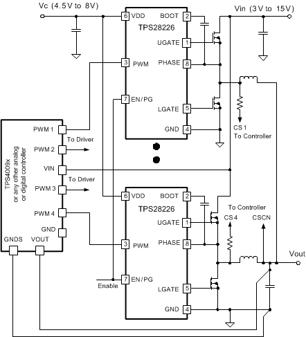 Figure 38. Multi-Phase Synchronous Buck Converter