SLUS791A July   2007  – September 2015 TPS28226

PRODUCTION DATA.  

  1. Features
  2. Applications
  3. Description
  4. Revision History
  5. Pin Configuration and Functions
  6. Specifications
    1. 6.1 Absolute Maximum Ratings
    2. 6.2 ESD Ratings
    3. 6.3 Recommended Operating Conditions
    4. 6.4 Thermal Information
    5. 6.5 Electrical Characteristics
    6. 6.6 Switching Characteristics
    7. 6.7 Typical Characteristics
  7. Detailed Description
    1. 7.1 Overview
    2. 7.2 Functional Block Diagram
    3. 7.3 Feature Description
      1. 7.3.1 Undervoltage Lockout (UVLO)
      2. 7.3.2 Output Active Low
      3. 7.3.3 Enable/Power Good
      4. 7.3.4 3-State Input
        1. 7.3.4.1 TPS28226 3-State Exit Mode
        2. 7.3.4.2 External Resistor Interference
      5. 7.3.5 Bootstrap Diode
      6. 7.3.6 Upper and Lower Gate Drivers
      7. 7.3.7 Dead-Time Control
      8. 7.3.8 Thermal Shutdown
    4. 7.4 Device Functional Modes
  8. Application and Implementation
    1. 8.1 Application Information
    2. 8.2 Typical Application
      1. 8.2.1 Design Requirements
      2. 8.2.2 Detailed Design Procedure
        1. 8.2.2.1 Four Phases Driven by TPS28226 Driver
        2. 8.2.2.2 Switching The MOSFETs
        3. 8.2.2.3 List of Materials
      3. 8.2.3 Application Curves
    3. 8.3 System Examples
  9. Power Supply Recommendations
  10. 10Layout
    1. 10.1 Layout Guidelines
    2. 10.2 Layout Example
  11. 11Device and Documentation Support
    1. 11.1 Device Support
      1. 11.1.1 Third-Party Products Disclaimer
    2. 11.2 Documentation Support
      1. 11.2.1 Related Documentation
    3. 11.3 Community Resources
    4. 11.4 Trademarks
    5. 11.5 Electrostatic Discharge Caution
    6. 11.6 Glossary
  12. 12Mechanical, Packaging, and Orderable Information

Package Options

Mechanical Data (Package|Pins)
Thermal pad, mechanical data (Package|Pins)
Orderable Information

5 Pin Configuration and Functions

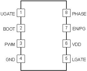
D Package
8-Pin SOIC
Top View
TPS28226 pin1_lus710.gif
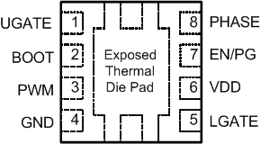
DRB Package
8-Pin VSON
Top View
TPS28226 pin2_lus710.gif

Pin Functions

PIN I/O DESCRIPTION
NAME NO.
SOIC VSON
BOOT 2 2 I/O Floating bootstrap supply pin for the upper gate drive. Connect the bootstrap capacitor between this pin and the Phase pin. The bootstrap capacitor provides the charge to turn on the upper MOSFET.
EN/PG 7 7 I/O Enable/power good input/output pin with 1-MΩ impedance. Connect this pin to High to enable and Low to disable the device. When disabled, the device draws less than 350-μA bias current. If the VDD is below UVLO threshold or over temperature shutdown occurs, this pin is internally pulled low.
GND 4 4 Ground pin. All signals are referenced to this node.
LGATE 5 5 O Lower gate drive sink and source output. Connect to the gate of the low-side power N-Channel MOSFET.
PHASE 8 8 I Connect this pin to the source of the upper MOSFET and the drain of the lower MOSFET. This pin provides a return path for the upper gate driver.
PWM 3 3 I The PWM signal is the control input for the driver. The PWM signal can enter three distinct states during operation, see the 3-state PWM Input section under DETAILED DESCRIPTION for further details. Connect this pin to the PWM output of the controller.
Thermal pad Exposed die pad Connect directly to the GND for better thermal performance and EMI.
UGATE 1 1 O Upper gate drive sink/source output. Connect to gate of high-side power N-Channel MOSFET.
VDD 6 6 I Connect this pin to a 5-V bias supply. Place a high quality bypass capacitor from this pin to GND.