SNVSB66A July   2018  – October 2021 TPS3431

PRODUCTION DATA  

  1. Features
  2. Applications
  3. Description
  4. Revision History
  5. Pin Configuration and Functions
  6. Specifications
    1. 6.1 Absolute Maximum Ratings
    2. 6.2 ESD Ratings
    3. 6.3 Recommended Operating Conditions
    4. 6.4 Thermal Information
    5. 6.5 Electrical Characteristics
    6. 6.6 Timing Requirements
    7. 6.7 Timing Diagrams
    8. 6.8 Typical Characteristics
  7. Detailed Description
    1. 7.1 Overview
    2. 7.2 Functional Block Diagram
    3. 7.3 Feature Description
      1. 7.3.1 Enable Input (EN) and Enable Output (ENOUT)
      2. 7.3.2 Watchdog Mode
        1. 7.3.2.1 CWD
        2. 7.3.2.2 Watchdog Input WDI
        3. 7.3.2.3 Watchdog Output WDO
        4. 7.3.2.4 SET1
    4. 7.4 Device Functional Modes
      1. 7.4.1 VDD is Below VPOR ( VDD < VPOR)
      2. 7.4.2 Above Power-On-Reset, But Less Than VDD(min) (VPOR ≤ VDD < VDD(min))
      3. 7.4.3 Normal Operation (VDD ≥ VDD(min))
  8. Application and Implementation
    1. 8.1 Application Information
      1. 8.1.1 CWD Functionality
        1. 8.1.1.1 Factory-Programmed Timing Options
        2. 8.1.1.2 CWD Adjustable Capacitor Watchdog Timeout
    2. 8.2 Typical Application
      1. 8.2.1 Design 1 Requirements
      2. 8.2.2 Detailed Design 1 Procedure
        1. 8.2.2.1 Calculating WDO Pullup Resistor Design 1
        2. 8.2.2.2 Setting the Watchdog Design 1
      3. 8.2.3 Application Curves Design 1
    3. 8.3 Programmable Application
      1. 8.3.1 Design 2 Requirements
      2. 8.3.2 Detailed Design 2 Procedure
        1. 8.3.2.1 Calculating WDO Pullup Resistor Design 2
        2. 8.3.2.2 Setting the Watchdog Design 2
        3. 8.3.2.3 Watchdog Disabled During Initialization Period Design 2
        4. 8.3.2.4 Programmable Disable Feature Design 2
      3. 8.3.3 Application Curves Design 2
  9. Power Supply Recommendations
  10. 10Layout
    1. 10.1 Layout Guidelines
    2. 10.2 Layout Example
  11. 11Device and Documentation Support
    1. 11.1 Device Support
    2. 11.2 Documentation Support
      1. 11.2.1 Related Documentation
    3. 11.3 Receiving Notification of Documentation Updates
    4. 11.4 Support Resources
    5. 11.5 Trademarks
    6. 11.6 Electrostatic Discharge Caution
    7. 11.7 Glossary
  12. 12Mechanical, Packaging, and Orderable Information

Package Options

Mechanical Data (Package|Pins)
Thermal pad, mechanical data (Package|Pins)
Orderable Information

Description

The TPS3431 is a standard programmable watchdog timer with an enable feature for a wide variety of applications. The watchdog timeout features a 15% accuracy, high-precision timing (–40°C to +125°C) and 2.5% typical at 25°C. The watchdog timeout can be programmed either by an external capacitor, or by factory-programmed default delay settings. The watchdog can be disabled via the Enable pin or the SET logic pins to avoid undesired watchdog timeouts during the development process.

The TPS3431 is available in a small 3.00-mm ×
3.00-mm, 8-pin VSON package.

Device Information(1)
PART NUMBER PACKAGE BODY SIZE (NOM)
TPS3431 VSON (8) 3.00 mm × 3.00 mm
For all available packages, see the orderable addendum at the end of the data sheet.
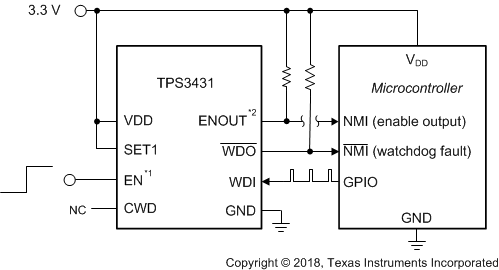
GUID-E9AE443C-308B-4440-A867-1FA555A3C907-low.gif
EN can also be left floating and is internally pulled-up to VDD
ENOUT can also be left floating or tied to WDO
Standard Watchdog Timer Circuit
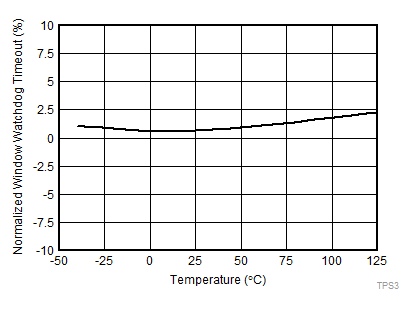
GUID-F67D9D92-3F0E-4C45-953E-0EB74DF8169D-low.gifNormalized Watchdog Timeout (tWD) Accuracy (SET1 = 1, CWD = NC)