SLVSGF1A october   2022  – june 2023 TPS3436-Q1

PRODUCTION DATA  

  1.   1
  2. Features
  3. Applications
  4. Description
  5. Revision History
  6. Device Comparison
  7. Pin Configuration and Functions
  8. Specifications
    1. 7.1 Absolute Maximum Ratings
    2. 7.2 ESD Ratings
    3. 7.3 Recommended Operating Conditions
    4. 7.4 Thermal Information
    5. 7.5 Electrical Characteristics
    6. 7.6 Timing Requirements
    7. 7.7 Switching Characteristics
    8. 7.8 Timing Diagrams
    9. 7.9 Typical Characteristics
  9. Detailed Description
    1. 8.1 Overview
    2. 8.2 Functional Block Diagrams
    3. 8.3 Feature Description
      1. 8.3.1 Window Watchdog Timer
        1. 8.3.1.1 tWC (Close Window) Timer
        2. 8.3.1.2 tWO (Open Window) Timer
        3. 8.3.1.3 Watchdog Enable Disable Operation
        4. 8.3.1.4 tSD Watchdog Start Up Delay
        5. 8.3.1.5 SET Pin Behavior
      2. 8.3.2 Manual RESET
      3. 8.3.3 WDO Output
    4. 8.4 Device Functional Modes
  10. Application and Implementation
    1. 9.1 Application Information
      1. 9.1.1 Output Assert Delay
        1. 9.1.1.1 Factory-Programmed Output Assert Delay Timing
        2. 9.1.1.2 Adjustable Capacitor Timing
      2. 9.1.2 Watchdog Window Functionality
        1. 9.1.2.1 Factory-Programmed Timing Options
        2. 9.1.2.2 Adjustable Capacitor Timing
    2. 9.2 Typical Applications
      1. 9.2.1 Design 1: Monitoring a Microcontroller Watchdog During Operational and Sleep Modes
        1. 9.2.1.1 Design Requirements
        2. 9.2.1.2 Detailed Design Procedure
          1. 9.2.1.2.1 Determining Window Timings During Operation and Sleep Modes
          2. 9.2.1.2.2 Meeting the Output Assert Delay
          3. 9.2.1.2.3 Calculating the WDO Pullup Resistor
    3. 9.3 Power Supply Recommendations
    4. 9.4 Layout
      1. 9.4.1 Layout Guidelines
      2. 9.4.2 Layout Example
  11. 10Device and Documentation Support
    1. 10.1 Receiving Notification of Documentation Updates
    2. 10.2 Support Resources
    3. 10.3 Trademarks
    4. 10.4 Electrostatic Discharge Caution
    5. 10.5 Glossary
  12. 11Mechanical, Packaging, and Orderable Information

Package Options

Mechanical Data (Package|Pins)
Thermal pad, mechanical data (Package|Pins)
Orderable Information
Calculating the WDO Pullup Resistor

The TPS3436-Q1 uses an open-drain configuration for the WDO circuit, as shown in Figure 9-2. When the FET is off, the resistor pulls the drain of the transistor to VDD and when the FET is turned on, the FET attempts to pull the drain to ground, thus creating an effective resistor divider. The resistors in this divider must be chosen to ensure that VOL is below its maximum value. To choose the proper pullup resistor, there are three key specifications to keep in mind: the pullup voltage (VPU), the recommended maximum WDO pin current (IRST), and VOL. The maximum VOL is 0.3 V, meaning that the effective resistor divider created must be able to bring the voltage on the reset pin below 0.3 V with IRST kept below 2 mA for VDD ≥ 3 V and 500 μA for VDD = 1.5 V. For this example, with a VPU =VDD = 1.5 V, a resistor must be chosen to keep IRST below 500 μA because this value is the maximum consumption current allowed. To ensure this specification is met, a pullup resistor value of 10 kΩ was selected, which sinks a maximum of 180 μA when WDO is asserted.
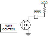
GUID-222FA4BF-5EE7-44BC-B8CA-C47795549DD2-low.pngFigure 9-2 Open-Drain RESET Configuration