SNVSBJ1E october   2020  – august 2023 TPS37

PRODUCTION DATA  

  1.   1
  2. Features
  3. Applications
  4. Description
  5. Revision History
  6. Device Comparison
  7. Pin Configuration and Functions
  8. Specifications
    1. 7.1 Absolute Maximum Ratings
    2. 7.2 ESD Ratings
    3. 7.3 Recommended Operating Conditions
    4. 7.4 Thermal Information
    5. 7.5 Electrical Characteristics
    6. 7.6 Timing Requirements
    7. 7.7 Timing Diagrams
    8. 7.8 Typical Characteristics
  9. Detailed Description
    1. 8.1 Overview
    2. 8.2 Functional Block Diagram
    3. 8.3 Feature Description
      1. 8.3.1 Input Voltage (VDD)
        1. 8.3.1.1 Undervoltage Lockout (VPOR < VDD < UVLO)
        2. 8.3.1.2 Power-On Reset (VDD < VPOR )
      2. 8.3.2 SENSE
        1. 8.3.2.1 SENSE Hysteresis
      3. 8.3.3 Output Logic Configurations
        1. 8.3.3.1 Open-Drain
        2. 8.3.3.2 Push-Pull
        3. 8.3.3.3 Active-High (RESET)
        4. 8.3.3.4 Active-Low (RESET)
      4. 8.3.4 User-Programmable Reset Time Delay
        1. 8.3.4.1 Reset Time Delay Configuration
      5. 8.3.5 User-Programmable Sense Delay
        1. 8.3.5.1 Sense Time Delay Configuration
      6. 8.3.6 Manual RESET (CTR1 / MR) and (CTR2 / MR) Input
  10. Device Functional Modes
  11. 10Application and Implementation
    1. 10.1 Adjustable Voltage Thresholds
      1. 10.1.1 Application Curves
    2. 10.2 Application Information
      1. 10.2.1 Typical Application
        1. 10.2.1.1 Design 1: High Voltage – Fast AC Signal Monitoring For Power Fault Detection
          1. 10.2.1.1.1 Design Requirements
          2. 10.2.1.1.2 Detailed Design Procedure
    3. 10.3 Power Supply Recommendations
      1. 10.3.1 Power Dissipation and Device Operation
    4. 10.4 Layout
      1. 10.4.1 Layout Guidelines
      2. 10.4.2 Layout Example
      3. 10.4.3 Creepage Distance
  12. 11Device and Documentation Support
    1. 11.1 Device Nomenclature
    2. 11.2 Support Resources
    3. 11.3 Trademarks
    4. 11.4 Electrostatic Discharge Caution
    5. 11.5 Glossary

Package Options

Mechanical Data (Package|Pins)
Thermal pad, mechanical data (Package|Pins)
Orderable Information

Manual RESET (CTR1 / MR) and (CTR2 / MR) Input

The manual reset input allows a processor or other logic circuits to initiate a reset. In this section MR is a generic reference to (CTR1 / MR) and (CTR2 / MR). A logic low on MR causes RESET1 to assert on reset output. After MR is left floating, RESET1 will release the reset if the voltage at SENSE1 pin is at nominal voltage. MR should not be driven high, this pin should be left floating or connected to a capacitor to GND, this pin can be left unconnected if is not used.

If the logic driving the MR cannot tri-state (floating and GND) then a logic-level FET should be used as illustrated in Figure 8-8.
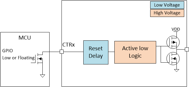
GUID-AFBB54A8-B5BE-4496-8FAD-C4D1DAD41720-low.gif Figure 8-8 Manual Reset Implementation
GUID-20210112-CA0I-BXR7-8D9D-XXQHS2J8SBPN-low.svg Figure 8-9 Manual Reset Timing Diagram
Table 8-3 MR Functional Table
MR SENSE ON NOMINAL VOLTAGE RESET STATUS
Low Yes Reset asserted
Floating Yes Fast reset release when SENSE voltage goes back to nominal voltage
Capacitor Yes Programmable reset time delay
High Yes NOT Recommended