SBVS251A January 2015 – February 2024 TPS3702
PRODUCTION DATA
- 1
- 1 Features
- 2 Applications
- 3 Description
- 4 Pin Configuration and Functions
- 5 Specifications
- 6 Detailed Description
- 7 Application and Implementation
- 8 Power Supply Recommendations
- 9 Layout
- 10Device and Documentation Support
- 11Revision History
- 12Mechanical, Packaging, and Orderable Information
Package Options
Mechanical Data (Package|Pins)
- DDC|6
Thermal pad, mechanical data (Package|Pins)
Orderable Information
3 Description
The TPS3702 is an integrated overvoltage and undervoltage window voltage detector in a small SOT-6 package. This highly accurate voltage detector is an excellent choice for systems that operate on low-voltage supply rails and have narrow margin supply tolerances. Low threshold hysteresis options of 0.55% and 1.0% prevent false reset signals when the monitored voltage supply is in the normal range of operation. Internal glitch immunity and noise filters further eliminate false resets resulting from erroneous signals.
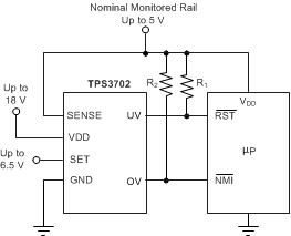
The TPS3702 does not require any external resistors for setting overvoltage and undervoltage reset thresholds, which further increases overall accuracy and reduces solution size and cost. The SET pin is used to select between the two available threshold voltages designed into each device. A separate SENSE input pin and VDD pin allow for the redundancy sought by safety-critical and high-reliability systems. This device also features independent reset outputs for the OV and UV pins; as a result of the open-drain configuration, UV and OV can be tied together.
This device has a low typical quiescent current specification of 7µA and is qualified for use over the industrial temperature range of –40°C to 125°C.
 Typical Application Circuit