SBVS251A January   2015  – February 2024 TPS3702

PRODUCTION DATA  

  1.   1
  2. Features
  3. Applications
  4. Description
  5. Pin Configuration and Functions
  6. Specifications
    1. 5.1 Absolute Maximum Ratings
    2. 5.2 ESD Ratings
    3. 5.3 Recommended Operating Conditions
    4. 5.4 Thermal Information
    5. 5.5 Electrical Characteristics
    6. 5.6 Timing Requirements
    7. 5.7 Typical Characteristics
  7. Detailed Description
    1. 6.1 Overview
    2. 6.2 Functional Block Diagram
    3. 6.3 Feature Description
      1. 6.3.1 Input (SENSE)
      2. 6.3.2 Outputs (UV, OV)
      3. 6.3.3 User-Configurable Accuracy Band (SET)
    4. 6.4 Device Functional Modes
      1. 6.4.1 Normal Operation (VDD > UVLO)
      2. 6.4.2 Undervoltage Lockout (V(POR) < VDD < UVLO)
      3. 6.4.3 Power-On Reset (VDD < V(POR))
  8. Application and Implementation
    1. 7.1 Application Information
      1. 7.1.1 Window Voltage Detector Considerations
      2. 7.1.2 Input and Output Configurations
      3. 7.1.3 Immunity to SENSE Pin Voltage Transients
    2. 7.2 Typical Application
      1. 7.2.1 Design Requirements
      2. 7.2.2 Detailed Design Procedure
      3. 7.2.3 Application Curves
  9. Power Supply Recommendations
  10. Layout
    1. 9.1 Layout Guidelines
    2. 9.2 Layout Example
  11. 10Device and Documentation Support
    1. 10.1 Device Support
      1. 10.1.1 Development Support
        1. 10.1.1.1 Evaluation Module
      2. 10.1.2 Device Nomenclature
    2. 10.2 Documentation Support
      1. 10.2.1 Related Documentation
    3. 10.3 Support Resources
    4. 10.4 Trademarks
    5. 10.5 Electrostatic Discharge Caution
    6. 10.6 Glossary
  12. 11Revision History
  13. 12Mechanical, Packaging, and Orderable Information

Package Options

Mechanical Data (Package|Pins)
Thermal pad, mechanical data (Package|Pins)
Orderable Information

Typical Characteristics

At TJ = 25°C, VDD = 3V, and RPU = 10kΩ, unless otherwise noted.

GUID-4DD625AA-865E-47CC-B6E4-7D39CC57C783-low.png
Performance is across VDD with SET high or low
Figure 5-2 Undervoltage Accuracy vs Temperature
GUID-9CDF383A-58C7-4571-8F10-015AFE6F4E36-low.gif
Performance is across VDD with SET high or low
Figure 5-4 Undervoltage Accuracy Distribution
GUID-CDA1586E-5E24-48F9-B933-1C61CECBD953-low.png
Figure 5-6 Supply Current vs Supply Voltage
GUID-073061A6-37BE-4733-B5C0-01610E0BA92F-low.png
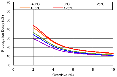
SENSE transitions from high to low
Figure 5-8 Undervoltage Propagation Delay vs Overdrive
GUID-23EA8C0B-C105-4C8C-9FCA-69A04076DE32-low.png
SENSE transitions from low to high
Figure 5-10 Undervoltage Propagation Delay vs Overdrive
GUID-27612D0F-A57C-411E-A252-22CC028E5528-low.png
VDD = 1.8V
Figure 5-12 Low-Level Output Voltage vs Output Current
GUID-A22CDB73-406A-4801-8C95-B8DD8B3BE413-low.png
Figure 5-14 SET Threshold vs Temperature
GUID-13B669AD-ECC8-4A53-AE25-CD2F23565738-low.png
Performance is across VDD with SET high or low
Figure 5-3 Overvoltage Accuracy vs Temperature
GUID-05F89CF8-1875-4A6B-B7DB-3792F7C770B3-low.gif
Performance is across VDD with SET high or low
Figure 5-5 Overvoltage Accuracy Distribution
GUID-E4A774C9-CCEC-4620-9142-CFD5A3380E00-low.png
Figure 5-7 Undervoltage Lockout Threshold vs Temperature
GUID-B63F0B63-D5EC-4DD4-88AF-E5D347D6B606-low.png
SENSE transitions from low to high
Figure 5-9 Overvoltage Propagation Delay vs Overdrive
GUID-17B4C3B7-C03F-4706-9CCE-EB645106E024-low.png
SENSE transitions from high to low
Figure 5-11 Overvoltage Propagation Delay vs Overdrive
GUID-AC044817-AC39-47D8-AB59-344F12CC38B9-low.png
VDD = 18V
Figure 5-13 Low-Level Output Voltage vs Output Current