SBVS251A January 2015 – February 2024 TPS3702
PRODUCTION DATA
- 1
- 1 Features
- 2 Applications
- 3 Description
- 4 Pin Configuration and Functions
- 5 Specifications
- 6 Detailed Description
- 7 Application and Implementation
- 8 Power Supply Recommendations
- 9 Layout
- 10Device and Documentation Support
- 11Revision History
- 12Mechanical, Packaging, and Orderable Information
Package Options
Mechanical Data (Package|Pins)
- DDC|6
Thermal pad, mechanical data (Package|Pins)
Orderable Information
6.3.3 User-Configurable Accuracy Band (SET)
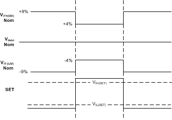
The TPS3702 has a remarkable feature allowing each device to be set for one of two accuracy bands, Table 10-1 describes the available accuracy bands with nominal thresholds ranging from ±2% to ±10% of the monitored rail nominal voltage. Forcing the voltage on the SET pin above the high-level SET pin input voltage, VIH(SET), sets the thresholds for the tighter window whereas forcing the voltage on the SET pin below the low-level SET pin input voltage, VIL(SET), sets the thresholds for the wider window.
Using the TPS3702Cxxx as an example, when VSET ≥ VIH(SET) the nominal thresholds are set to ±4% (see Figure 6-1). Thus, when the positive-going and negative-going threshold accuracy is accounted for, the device outputs an active low signal for voltage excursions outside a ±4.9% band (worst case), which is calculated by taking the nominal threshold percentage for that given part number and adding that value to the threshold accuracy found in the Section 5 section. Similarly, when VSET ≤ VIL(SET), the nominal thresholds are set to ±9% and the device outputs an active low signal for voltage excursions outside the ±9.9% band (worst case).
The ability for the user to change the accuracy band allows a system to programmatically change the accuracy band during certain conditions. One example is during system start up when the monitored voltage can be slightly outside the typical accuracy specifications but a reset signal is not desired. In this case, VSET can be set below VIL(SET) to detect voltage excursions outside the 10% band and, after the system is fully started up, VSET can be pulled higher than VIH(SET), thus tightening the band to ±5%.
 Figure 6-1 TPS3702Cxxx User-Configurable Accuracy Bands
Another benefit of allowing the user to change the accuracy band is the reduction in qualification costs. Users who have multiple rail monitoring needs (such as some rails that must be within ±5% of the nominal voltage and other rails that must be within ±10% of the same nominal voltage) benefit by only having to spend the time and money qualifying one device instead of two.