SBVS344D November 2018 – March 2021 TPS3703-Q1
PRODUCTION DATA
- 1 Features
- 2 Applications
- 3 Description
- 4 Revision History
- 5 Device Comparison
- 6 Pin Configuration and Functions
- 7 Specifications
- 8 Detailed Description
- 9 Application and Implementation
- 10Power Supply Recommendations
- 11Layout
- 12Device and Documentation Support
- 13Mechanical, Packaging, and Orderable Information
Package Options
Mechanical Data (Package|Pins)
- DSE|6
Thermal pad, mechanical data (Package|Pins)
Orderable Information
6 Pin Configuration and Functions
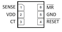
 Figure 6-1 DSE
Package,6-Pin WSON,Top View
Figure 6-1 DSE
Package,6-Pin WSON,Top ViewTable 6-1 Pin Functions
| PIN | I/O | DESCRIPTION | |
|---|---|---|---|
| NO. | NAME | ||
| 1 | SENSE | I | Input for the monitored supply voltage rail. When the SENSE voltage goes above the overvoltage threshold or below the undervoltage threshold, the RESET pin is driven low. Connect to VDD pin if monitoring VDD supply voltage. |
| 2 | VDD | I | Supply voltage input pin. Good analog design practice is to place a 0.1-μF ceramic capacitor close to this pin. |
| 3 | CT | I | Capacitor time delay pin. The CT pin offers two fixed time delays by connecting CT pin to VDD or leaving it floating. Delay time can be programmed by connecting an external capacitor reference to ground. |
| 4 | RESET | O | Active-low, open-drain output. This pin goes low when the SENSE voltage rises above the internally overvoltage threshold (VIT+) or below the undervoltage threshold (VIT–). See the timing diagram in Figure 8-2 for more details. Connect this pin to a pull-up resistor terminated to the desired pull-up voltage. |
| 5 | GND | — | Ground |
| 6 | MR | I | Manual reset (MR), pull this pin to a logic low (VMR_L) to assert a reset signal . After the MR pin is deasserted the output goes high after the reset delay time(tD) expires. MR can be left floating when not in use. |