SNVSBS9C March   2021  – May 2024 TPS3704-Q1

PRODUCTION DATA  

  1.   1
  2. Features
  3. Applications
  4. Description
  5. Device Nomenclature
  6. Pin Configuration and Functions
  7. Specifications
    1. 6.1 Absolute Maximum Ratings
    2. 6.2 ESD Ratings
    3. 6.3 Recommended Operating Conditions
    4. 6.4 Thermal Information
    5. 6.5 Electrical Characteristics
    6. 6.6 Timing Requirements
    7. 6.7 Timing Diagrams
    8. 6.8 Typical Characteristics
  8. Detailed Description
    1. 7.1 Overview
    2. 7.2 Functional Block Diagrams
    3. 7.3 Feature Description
      1. 7.3.1 VDD
      2. 7.3.2 SENSEx Input
        1. 7.3.2.1 Immunity to SENSEx Pins Voltage Transients
          1. 7.3.2.1.1 SENSEx Hysteresis
      3. 7.3.3 RESETx/RESETx
    4. 7.4 Device Functional Modes
      1. 7.4.1 Normal Operation (VDD > VDD(MIN))
      2. 7.4.2 Undervoltage Lockout (VPOR < VDD < UVLO)
      3. 7.4.3 Power-On Reset (VDD < VPOR)
  9. Application and Implementation
    1. 8.1 Application Information
      1. 8.1.1 Voltage Threshold Accuracy
      2. 8.1.2 Adjustable Voltage Thresholds
    2. 8.2 Typical Applications
      1. 8.2.1 Design 1: Multi-Rail Window Monitoring for Microcontroller Power Rails
        1. 8.2.1.1 Design Requirements
        2. 8.2.1.2 Detailed Design Procedure
      2. 8.2.2 Design 2: Manual Self-Test Option for Enhanced Functional Safety Use Cases
        1. 8.2.2.1 Design Requirements
        2. 8.2.2.2 Detailed Design Procedure
      3. 8.2.3 Application Curves
    3. 8.3 Power Supply Recommendations
      1. 8.3.1 Power Supply Guidelines
    4. 8.4 Layout
      1. 8.4.1 Layout Guidelines
      2. 8.4.2 Layout Example
  10. Device and Documentation Support
    1. 9.1 Device Nomenclature
    2. 9.2 Receiving Notification of Documentation Updates
    3. 9.3 Support Resources
    4. 9.4 Trademarks
    5. 9.5 Electrostatic Discharge Caution
    6. 9.6 Glossary
  11. 10Revision History
  12. 11Mechanical, Packaging, and Orderable Information

Package Options

Mechanical Data (Package|Pins)
Thermal pad, mechanical data (Package|Pins)
Orderable Information

Typical Characteristics

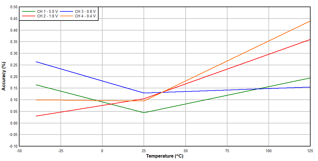
Typical characteristics show the typical performance of the TPS3704x-Q1 device. Test conditions are TA = 25°C, VDD = 3.3V, and Rpull-upx = 10kΩ, CLOAD = 50pF, unless otherwise noted.
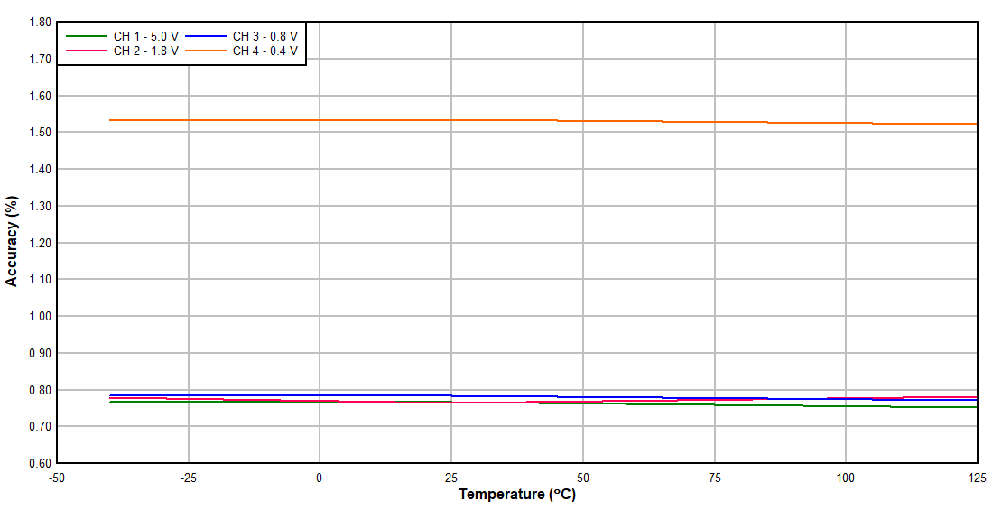
TPS3704-Q1 Undervoltage
            Accuracy vs TemperatureFigure 6-3 Undervoltage Accuracy vs Temperature
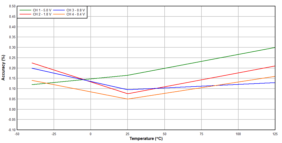
TPS3704-Q1 Undervoltage
            Hysteresis Voltage Accuracy vs TemperatureFigure 6-5 Undervoltage Hysteresis Voltage Accuracy vs Temperature
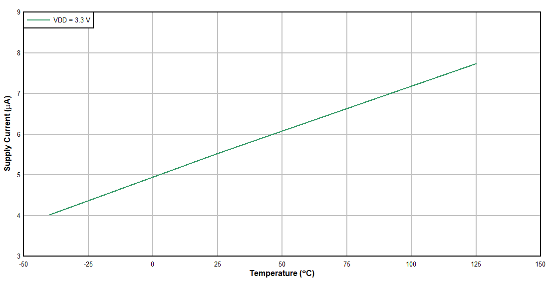
TPS3704-Q1 Supply Current
            vs Temperature
Output ( RESETx Pin) = High
Figure 6-7 Supply Current vs Temperature
TPS3704-Q1 Low-Level CH 1
            Output Voltage vs RESET1 Current
VDD = 5V
Figure 6-9 Low-Level CH 1 Output Voltage vs RESET1 Current
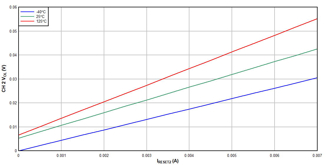
TPS3704-Q1 Low-Level CH 2
            Output Voltage vs RESET2 Current
VDD = 5V
Figure 6-11 Low-Level CH 2 Output Voltage vs RESET2 Current
TPS3704-Q1 Low-Level CH 3
            Output Voltage vs RESET3 Current
VDD = 5V
Figure 6-13 Low-Level CH 3 Output Voltage vs RESET3 Current
TPS3704-Q1 Low-Level CH 4
            Output Voltage vs RESET4 Current
VDD = 5V
Figure 6-15 Low-Level CH 4 Output Voltage vs RESET4 Current
TPS3704-Q1 SENSE1 Glitch
            Immunity (VIT+) vs Overdrive
VDD = 1.7V
Figure 6-17 SENSE1 Glitch Immunity (VIT+) vs Overdrive
TPS3704-Q1 SENSE1 Glitch
            Immunity (VIT+) vs Overdrive
VDD = 3.3V
Figure 6-19 SENSE1 Glitch Immunity (VIT+) vs Overdrive
TPS3704-Q1 SENSE1 Glitch
            Immunity (VIT+) vs Overdrive
VDD = 5V
Figure 6-21 SENSE1 Glitch Immunity (VIT+) vs Overdrive
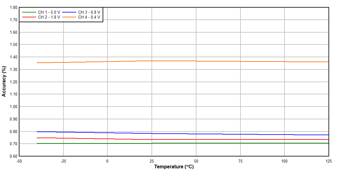
TPS3704-Q1 Overvoltage
            Accuracy vs TemperatureFigure 6-4 Overvoltage Accuracy vs Temperature
TPS3704-Q1 Overvoltage
            Hysteresis Voltage Accuracy vs TemperatureFigure 6-6 Overvoltage Hysteresis Voltage Accuracy vs Temperature
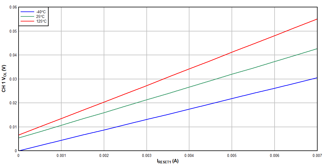
TPS3704-Q1 Low-Level CH 1
            Output Voltage vs RESET1 Current
VDD = 1.7V
Figure 6-8 Low-Level CH 1 Output Voltage vs RESET1 Current
TPS3704-Q1 Low-Level CH 2
            Output Voltage vs RESET2 Current
VDD = 1.7V
Figure 6-10 Low-Level CH 2 Output Voltage vs RESET2 Current
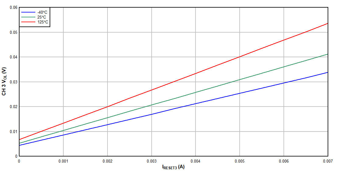
TPS3704-Q1 Low-Level CH 3
            Output Voltage vs RESET3 Current
VDD = 1.7V
Figure 6-12 Low-Level CH 3 Output Voltage vs RESET3 Current
TPS3704-Q1 Low-Level CH 4
            Output Voltage vs RESET4 Current
VDD = 1.7V
Figure 6-14 Low-Level CH 4 Output Voltage vs RESET4 Current
TPS3704-Q1 SENSE1 Glitch
            Immunity (VIT-) vs Overdrive
VDD = 1.7V
Figure 6-16 SENSE1 Glitch Immunity (VIT-) vs Overdrive
TPS3704-Q1 SENSE1 Glitch
            Immunity (VIT-) vs Overdrive
VDD = 3.3V
Figure 6-18 SENSE1 Glitch Immunity (VIT-) vs Overdrive
TPS3704-Q1 SENSE1 Glitch
            Immunity (VIT-) vs Overdrive
VDD = 5V
Figure 6-20 SENSE1 Glitch Immunity (VIT-) vs Overdrive